Thermally-enhanced multi-hole semiconductor package

a semiconductor and multi-hole technology, applied in semiconductor devices, semiconductor/solid-state device details, electrical devices, etc., can solve the problems of encapsulant bleeding onto the heat dissipation surface of the internal heat sink, chip failure, package warpage, etc., and achieves strong adhesion and high rigidity.

Inactive Publication Date: 2009-09-24
POWERTECH TECHNOLOGY
View PDF6 Cites 24 Cited by
  • Summary
  • Abstract
  • Description
  • Claims
  • Application Information

AI Technical Summary

Benefits of technology

[0004]The main purpose of the present invention is to provide a thermal-enhanced multi-hole semiconductor package by using the alignment bars of an internal heat sink aligned with and inserted into the alignment holes of a substrate. The aligned internal heat sink can be firmly held with a small amount of adhesive or without any adhesive. After packaging processes, the heat dissipation surface of the internal heat sink is free from the contaminations of the encapsulant and there is no gap between the internal heat sink and the chip for filling the encapsulant. The aligned internal heat sink becomes one assembly integrated with the chip and the substrate to enhance the heat dissipation efficiency and to reduce the substrate warpage, moreover, to avoid peeling of the internal heat sink.
[0005]The second purpose of the present invention is to provide a thermal-enhanced multi-hole semiconductor package to resolve the issues of shifting of an internal heat sink, extra internal stresses exerted on the chip, and higher heat resistance of an encapsulant.
[0006]The third purpose of the present invention is to provide a thermal-enhanced multi-hole semiconductor package to avoid encapsulant bleeding to the exposed heat dissipation surface of the internal heat sink by adjusting the coplanarity between the heat dissipation surface of the internal heat sink and the top surface of the encapsulant.
[0007]The fourth purpose of the present invention is to provide a thermal-enhanced multi-hole semiconductor package where the alignment bars of an internal heat sink are fully encapsulated by the encapsulant to provide higher bonding strengths and stronger adhesions with the substrate.
[0008]The fifth purpose of the present invention is to provide a thermal-enhanced multi-hole semiconductor package where the internal heat sink is fully adhered to the back surface of a chip to enhance heat dissipation efficiency.
[0010]The seventh purpose of the present invention is to provide a thermal-enhanced multi-hole semiconductor package to enhance the connection between the chip and the substrate to prevent delamination between the chip and the substrate.

Problems solved by technology

Just by the heat dissipation of chip itself is not enough to transfer the heat to the environment.
Therefore, the IC chip inside the encapsulant may be burned by considerable accumulated heat leading to chip failure, package warpage, and component peeling.
However, when the adhesive is cured or the solder is reflowed, the coplanarity between the heat dissipation surface of the internal heat sink and the top surface of the encapsulant can not be adjusted leading to bleeding of encapsulant onto the heat dissipation surface of the internal heat sink.
Furthermore, the encapsulant will flow into and fill the gaps between the internal heat sink and the chip leading to poor thermal conductivity.

Method used


Image

  • Thermally-enhanced multi-hole semiconductor package
  • Thermally-enhanced multi-hole semiconductor package
  • Thermally-enhanced multi-hole semiconductor package

Examples


first embodiment

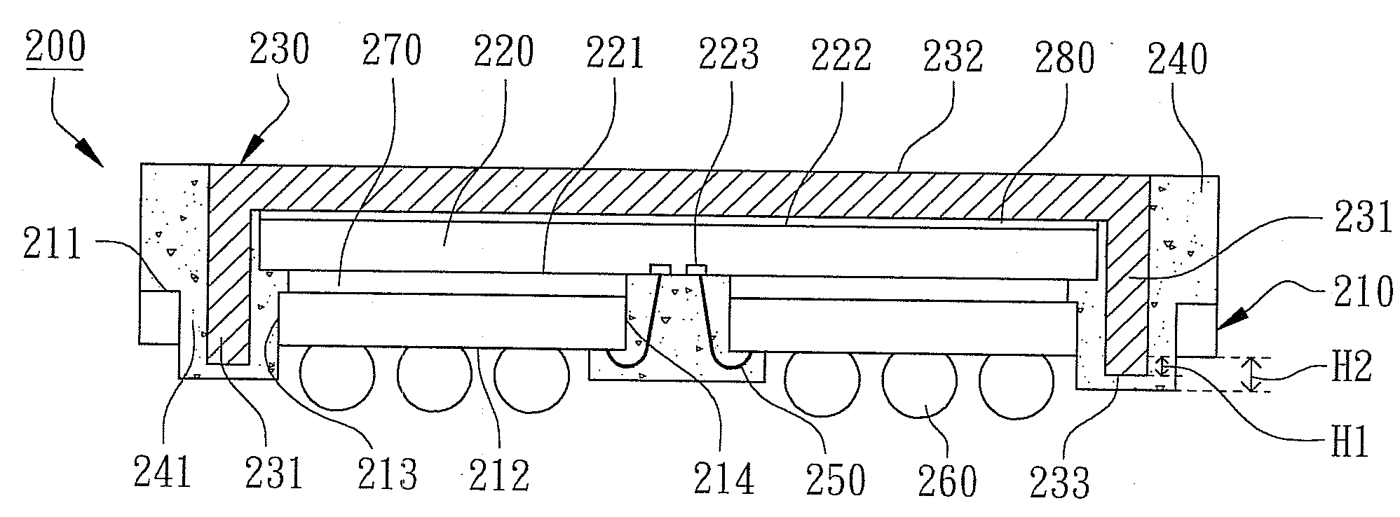
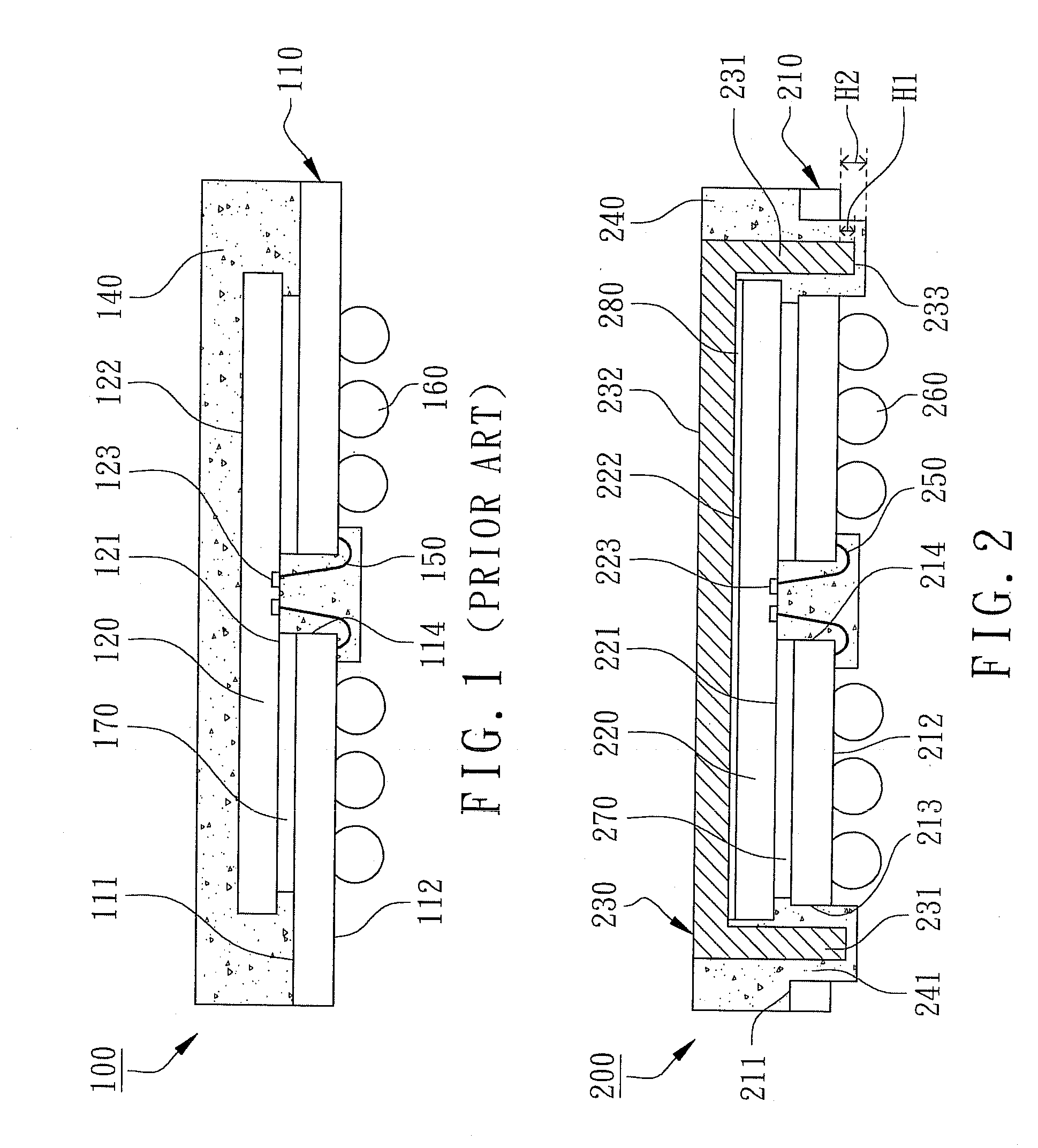
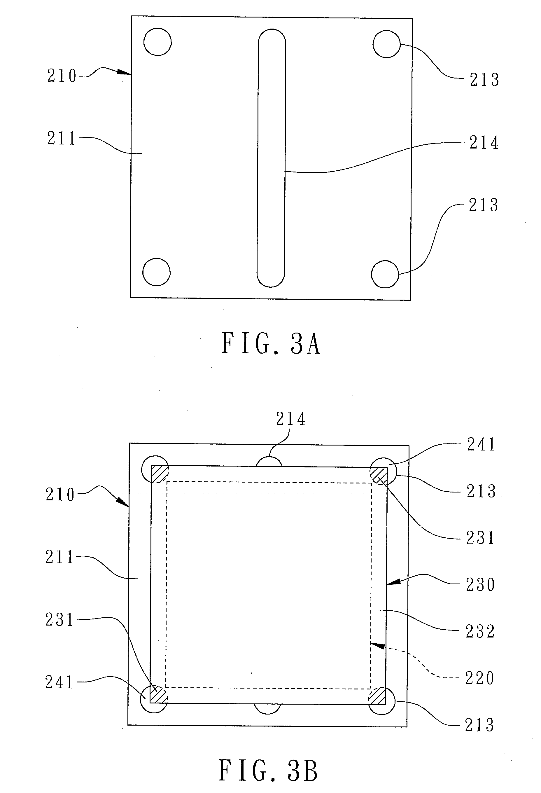
[0022]According to the present invention, as shown in FIG. 2, a thermal-enhanced multi-hole semiconductor package 200 primarily comprises a substrate 210, a chip 220, an internal heat sink 230, and an encapsulant 240. The substrate 210 has a top surface 211, a bottom surface 212, and a plurality of alignment holes 213 where the alignment holes 213 penetrates through the top surface 211 to the bottom surface 212. As shown in FIG. 3A, in the present embodiment, the alignment holes 213 include four corner holes adjacent to the four corners of the substrate 210. The substrate 210 further has a slot 214 located at a central line of the substrate 210. The slot 214 penetrates through the substrate 210 for passing through a plurality of electrical connecting components 250. In this embodiment, the substrate 210 is a printed circuit board including one or more circuit layers.

[0023]The chip 220 is attached to the top surface 211 of the substrate 210. As shown in FIG. 3B, both ends of the slot...

second embodiment

[0030]According to the present invention, another thermal-enhanced multi-hole semiconductor package 200 is revealed. As shown in FIG. 6, the thermal-enhanced multi-hole semiconductor package 300 primarily comprises a substrate 310, a chip 320, an internal heat sink 330 and an encapsulant 240. The substrate 310 has a top surface 311, a bottom surface 312, and a plurality of alignment holes 313. The chip 320 is disposed on the top surface 311 and a plurality of external terminals 360 such as solder balls are disposed on the bottom surface 312 for mounting to an external printed circuit board, not shown in the figure. The alignment holes 313 include four corner holes adjacent to the four corners of the substrate 310. As shown in FIG. 7, in the present embodiment, the alignment holes 313 further include at least two side holes adjacent to the two opposing sides of the substrate 310. As shown in FIG. 8, the chip 320 is attached to the top surface 311 of the substrate 310. As shown in FIG...


PUM


Abstract

A thermal-enhanced multi-hole semiconductor package is revealed, primarily comprising a substrate with a plurality of alignment holes, a chip disposed on the substrate, an internal heat sink attached to the chip, and an encapsulant. The internal hear sink has a plurality of alignment bars and a heat dissipation surface. The alignment bars are inserted into the alignment holes, but not fully occupying the alignment holes to provide a plurality of flowing channels therein. The encapsulant completely encapsulates the alignment bars through filling the flowing channels. Therefore, the internal heat sink can be aligned to the substrate and is integrally connected with the chip and the substrate utilizing a small amount of adhesive or without any adhesive to form a composite having high rigidity and strong adhesion.

Description

FIELD OF THE INVENTION[0001]The present invention relates to semiconductor devices, especially to thermal-enhanced multi-hole semiconductor packages.BACKGROUND OF THE INVENTION[0002]Conventionally, a chip is attached to a substrate and an encapsulant is formed on top of the substrate to encapsulate the chip to avoid external contaminations. As the advances of the semiconductor technologies and the increased functions of IC chips, the operations of an IC chip is faster and faster leading to higher chip temperatures. More and more heat will be cumulated in the encapsulant when the frequencies and the power of IC chip under operations are getting higher and higher. Just by the heat dissipation of chip itself is not enough to transfer the heat to the environment. Therefore, the IC chip inside the encapsulant may be burned by considerable accumulated heat leading to chip failure, package warpage, and component peeling.[0003]As shown in FIG. 1, a conventional window-type semiconductor pac...

Claims


Application Information

Patent Timeline
Patent Type & Authority Applications(United States)
IPC IPC(8): H01L23/367
CPCH01L23/13H01L23/3128H01L24/49H01L24/48H01L2924/15311H01L2924/14H01L23/4334H01L2224/48091H01L2224/4824H01L2224/49175H01L2924/00014H01L2924/00H01L2924/181H01L2224/45099H01L2224/45015H01L2924/207
Inventor YU, BING-SHUNHUNG, CHING-WEI
Owner POWERTECH TECHNOLOGY
Why Eureka
Try Eureka