
REO-Ge Multi-Junction Solar Cell

Inactive Publication Date: 2012-04-12
TRANSLUCENT
View PDF5 Cites 5 Cited by
  • Summary
  • Abstract
  • Description
  • Claims
  • Application Information

AI Technical Summary

Benefits of technology

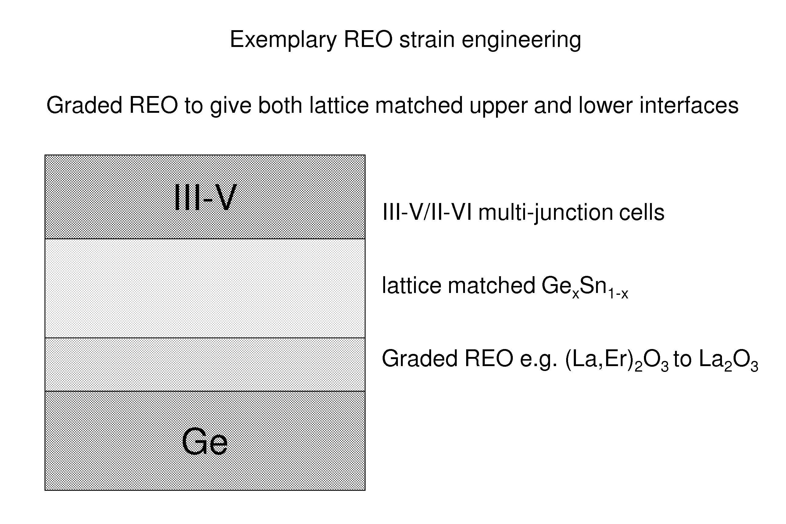
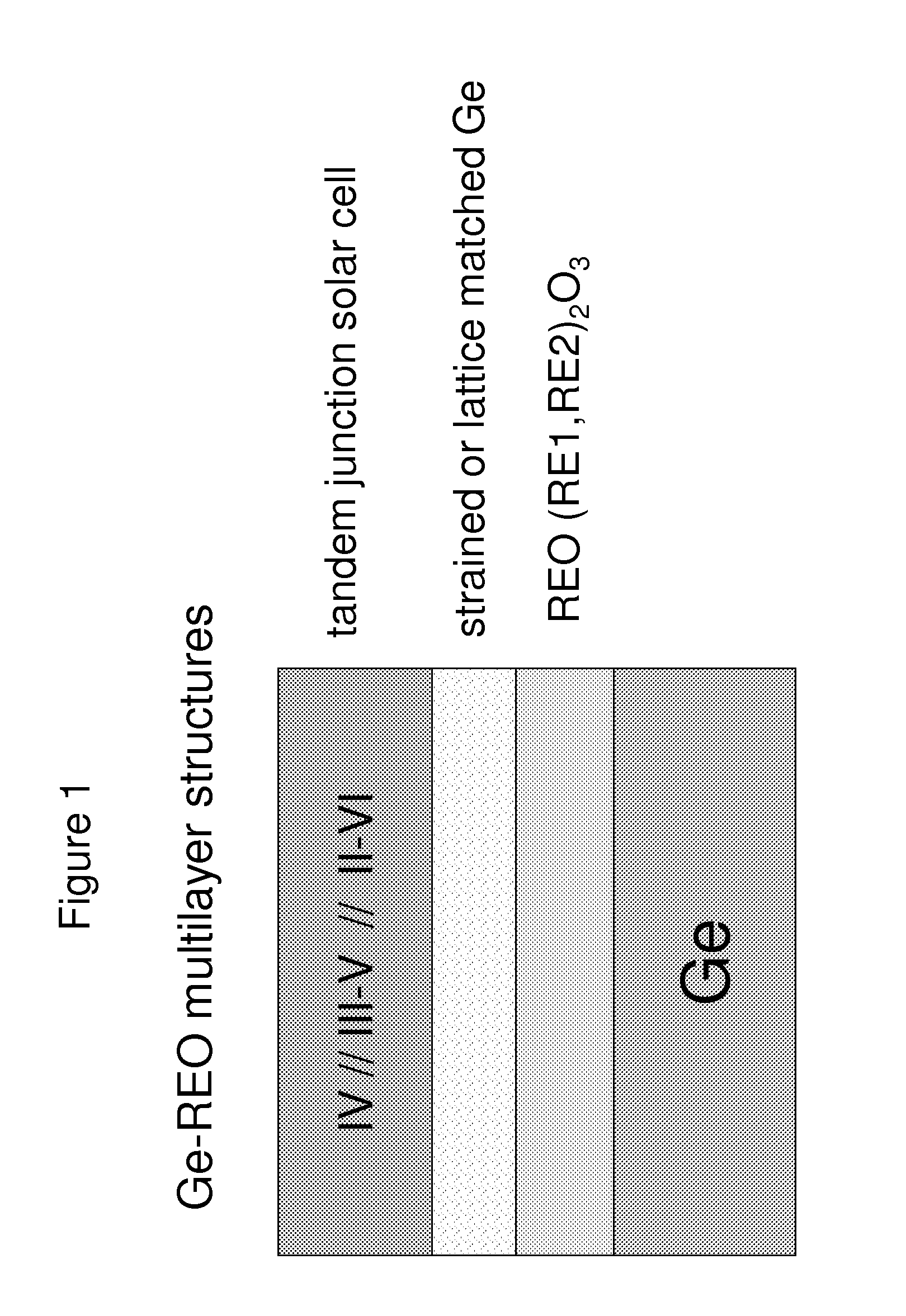
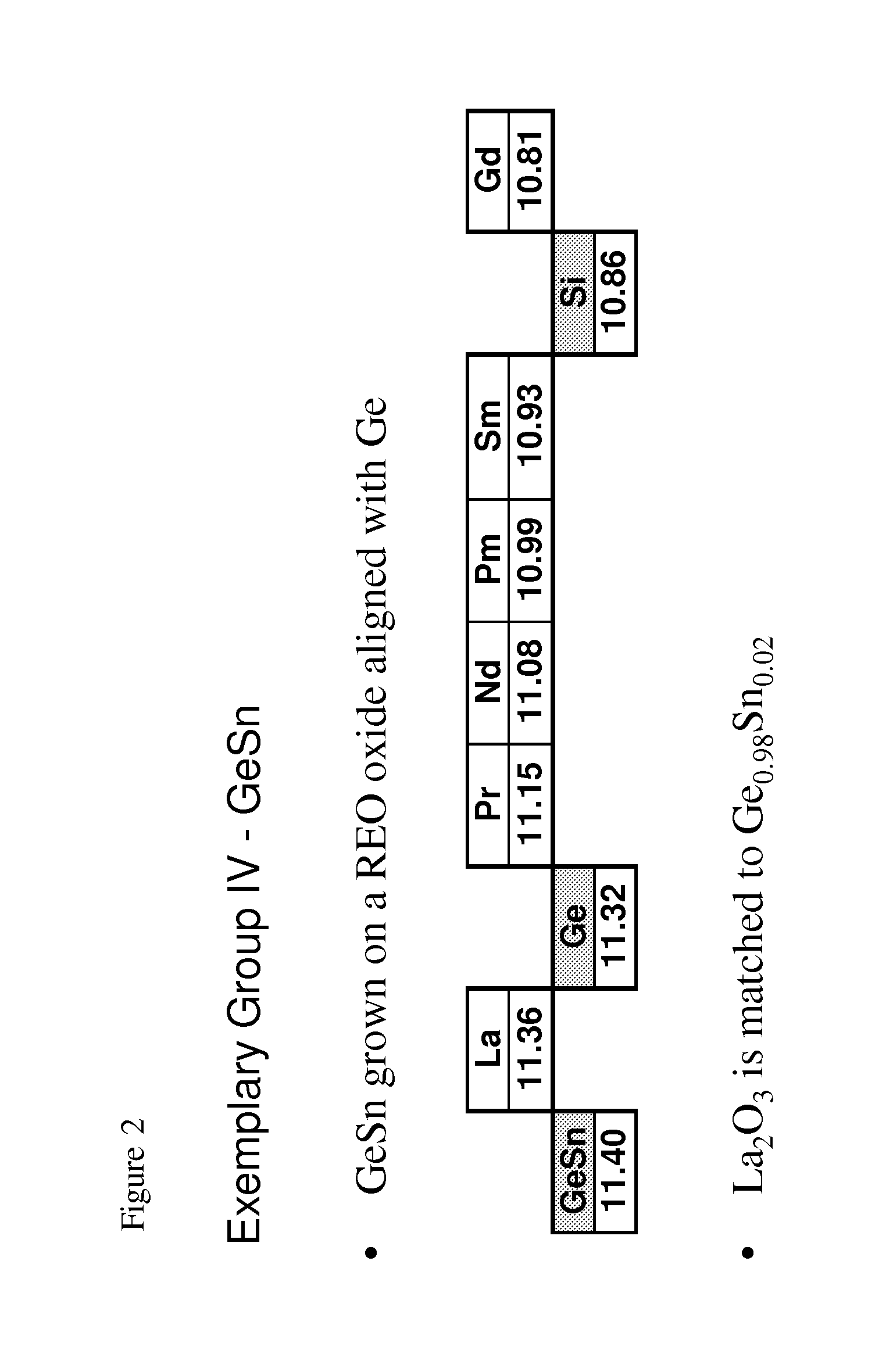
[0017]Triple junction materials are generally chosen from Group III-V materials, such as In, Ga, Al, As, P with the exact combinations tailored to specific energies but with restriction imposed by the choice of a germanium substrate or Ge support layer. By removing the restrictions of a germanium substrate, or support layer, new combinations of III-V alloys, and II-VI materials, are enabled. A lattice matched and / or engineered strained substrate or support layer with better current match and better band gap match to a broad selection of triple junction cell materials enables a higher efficiency multi-junction solar cell.

Problems solved by technology

Still, ultra-thin Si cells face a fundamental limitation.
Consequently, the industry is also approaching a fundamental limit when it comes to savings by reducing the Si thickness.

Method used


Image

  • REO-Ge Multi-Junction Solar Cell
  • REO-Ge Multi-Junction Solar Cell
  • REO-Ge Multi-Junction Solar Cell

Examples


Embodiment Construction

[0029]The instant invention discloses a structure to transition from a substrate of first composition to a semiconductor material of second composition, optionally, operable as a solar cell. A transition structure as defined herein comprises at least first rare earth based layer of third composition at a first surface and of fourth composition at a second surface; positioned such that the first surface is in contact with the substrate and the second surface is in contact with the semiconductor material; optionally, a Group IV based layer is between the rare earth based layer second surface and the semiconductor material. In some embodiments there are a plurality of rare earth based layers interleaved with Group IV based layers between a substrate and a semiconductor material of second composition.

[0030]FIG. 1 shows one embodiment of, optionally, a III-V multi-junction tandem solar cell over a lattice matched Group IV based layer, in this case a predominately Ge layer and a REO based...


PUM


Abstract

The invention relates to a semiconductor based structure for a device for converting radiation to electrical energy comprising various combinations of rare-earths and Group IV, III-V, and II-VI semiconductors and alloys thereof enabling enhanced performance including high radiation conversion efficiency.

Description

PRIORITY[0001]This application is a continuation of and claims priority from U.S. Ser. No. 13 / 020,766. U.S. Ser. No. 13 / 020,766 claims priority from U.S. Provisional Application 61 / 301,597 filed on Feb. 4, 2010 and is a continuation-in-part of Ser. No. 12 / 408,297, filed on Mar. 20, 2009, Ser. No. 12 / 510,977, filed on Jul. 28, 2009, and Ser. Nos. 12 / 619,637, 12 / 619,621, 12 / 619,549, all filed on Nov. 16, 2009 and claims priority from these applications, all included herein in their entirety by reference.CROSS REFERENCE TO RELATED APPLICATIONS[0002]Applications and patents, U.S.20050166834, Ser. Nos. 11 / 257,517, 11 / 257,597, 11 / 393,629, 11 / 472,087, 11 / 559,690, 11 / 599,691, 11 / 828,964, 11 / 858,838, 11 / 873,387 11 / 960,418, 11 / 961,938, 12 / 119,387, 60 / 820,438, 61 / 089,786, Ser. Nos. 12 / 029,443, 12 / 046,139, 12 / 111,568, 12 / 119,387, 12 / 171,200, 12 / 510,977, 12 / 632,741, 12 / 651,419, 12 / 890,537, 12 / 932,979, 13 / 015,315, 13 / 251,086, 61 / 298,896, 61 / 312,061, U.S. Pat. No. 6,734,453,U.S. Pat. No. 6,858,864...

Claims


Application Information

Patent Timeline
IPC IPC(8): H01L31/0352
CPCH01L31/072H01L31/0725H01L31/0735Y02E10/544H01L31/1812H01L31/1836H01L31/1852H01L31/0745
Inventor LEBBY, MICHAEL S.CLARK, ANDREWSMITH, ROBIN
Owner TRANSLUCENT
Learn More