
Flexible flat cable and method of manufacturing the same
a flat cable, flexible technology, applied in the direction of flat/ribbon cables, cables, insulation conductors/cables, etc., can solve the problems of lowering conductivity, manufacturing annealed or soft wires, etc., and achieve the effect of high conductivity and high bending durability
- Summary
- Abstract
- Description
- Claims
- Application Information
AI Technical Summary
Benefits of technology
Problems solved by technology
Method used
Image

Examples
embodiment mode 1
[0074]Table 1 lists results and relevant conditions of measuring conducted on the annealed dilute copper alloy materials by or pertinent to the present invention in terms of oxygen concentration, S concentration, Ti concentration, half-softening temperature, conductivity, dispersed particle size, and overall evaluation.
TABLE 12.6 mm diam.2.6 mm diam.WireAnnealedDispersedOxygenSulfurTitaniumHalf-softeningWireParticleExperimentalConcentrationConcentrationConcentrationTemperature.ConductivitySizeOverallMaterial(mass-ppm)(mass-ppm)(mass-ppm)(° C.)(% IACS)EvaluationEvaluationComparison1 to below 250215x101.7∘xMaterial 11 to below 257168x101.5∘x(through1 to below 2513160x100.9∘xsmall continuous1 to below 2515173x100.5∘xcasting apparatus)18190x99.6∘xComparison7 to 830164x102.2∘xMaterial 27 to 852157x102.1∘x(through SCR)Embodiment7 to 854148∘102.1∘∘Material 17 to 8510135∘102.2∘∘(through SCR)7 to 8513134∘102.4∘∘7 to 8520130∘102.2∘∘7 to 8525132∘102.0∘∘Comparison7 to 8537134∘101.1∘xMaterial 37...
embodiment 1
Embodiment Mode 2
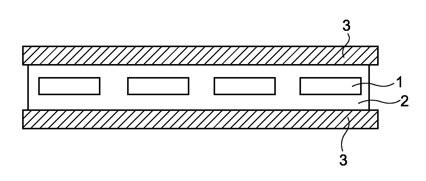
[0126]FIG. 13 is a cross-sectional view of a flexible flat cable in the embodiment. As illustrated in FIG. 13, the flexible flat cable has such a construction: that multiple number of flat conductors 1 by the present invention are arrayed flat on one common plane; that the array of the flat conductors is sandwiched between insulating films 3 from the direction of the flat-face of conductor, wherein one face of each of the insulating films has an adhesive layer 2 and the films are applied so that each of the adhesive layers 2 will be the inner face of the sandwich on the array of the conductors; and that the sandwich of the array of the flat conductors are fused by heating so that the constituting members are integrally one-bodied. The adhesive layer 2 is fused into one body in the area between the faces of the flat conductors 1 and in the area of both outer sides of the flat conductor. The following describes the embodiment of the present invention together with a c...
PUM
| Property | Measurement | Unit |
|---|---|---|
| temperature | aaaaa | aaaaa |
| temperature | aaaaa | aaaaa |
| temperature | aaaaa | aaaaa |
Abstract
Description
Claims
Application Information