Semiconductor device and method of fabricating the same

a technology of semiconductors and semiconductors, applied in the direction of semiconductor devices, basic electric elements, electrical equipment, etc., can solve the problems of affecting properties, generating a void within the shallow trench, and affecting the thickness of the substrate, so as to achieve constant width

Active Publication Date: 2012-05-03
KEY FOUNDRY CO LTD
View PDF8 Cites 164 Cited by
  • Summary
  • Abstract
  • Description
  • Claims
  • Application Information

AI Technical Summary

Problems solved by technology

In this case, however, undercut or undesirable roughness may appear due to excessive etching on the upper portion of the deep trench.
Further, dielectric material can be excessively deposited around the boundary between the deep and shallow trenches in the process of filling in dielectric material within the multi-depth trench, resulting in a generation of a void within the shallow trench.
The problems such as undercut, undesirable roughness, notch or void as mentioned above can affect the properties of the semiconductor device by affecting the stability of the semiconductor device.

Method used


Image

  • Semiconductor device and method of fabricating the same
  • Semiconductor device and method of fabricating the same
  • Semiconductor device and method of fabricating the same

Examples


Embodiment Construction

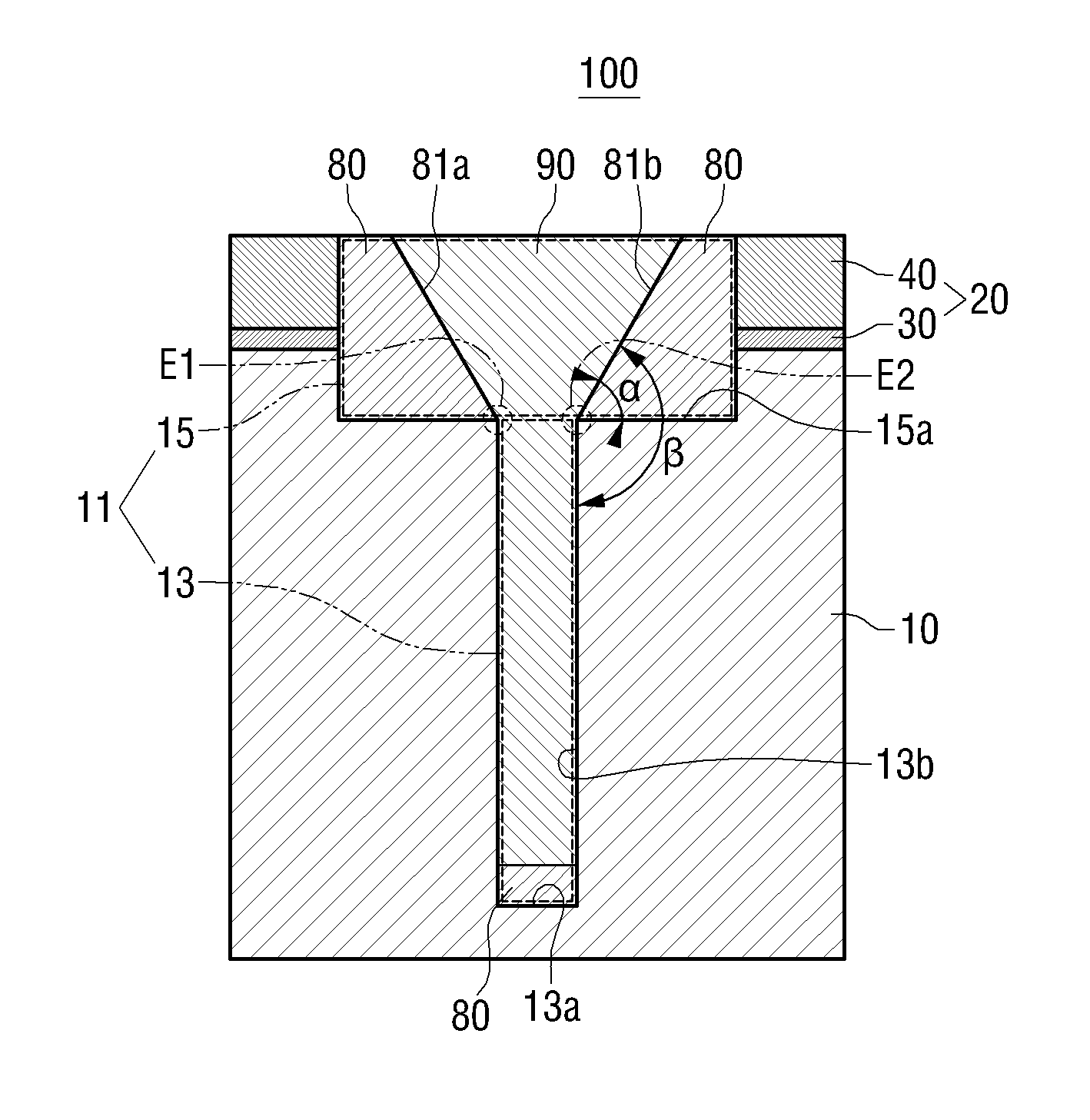
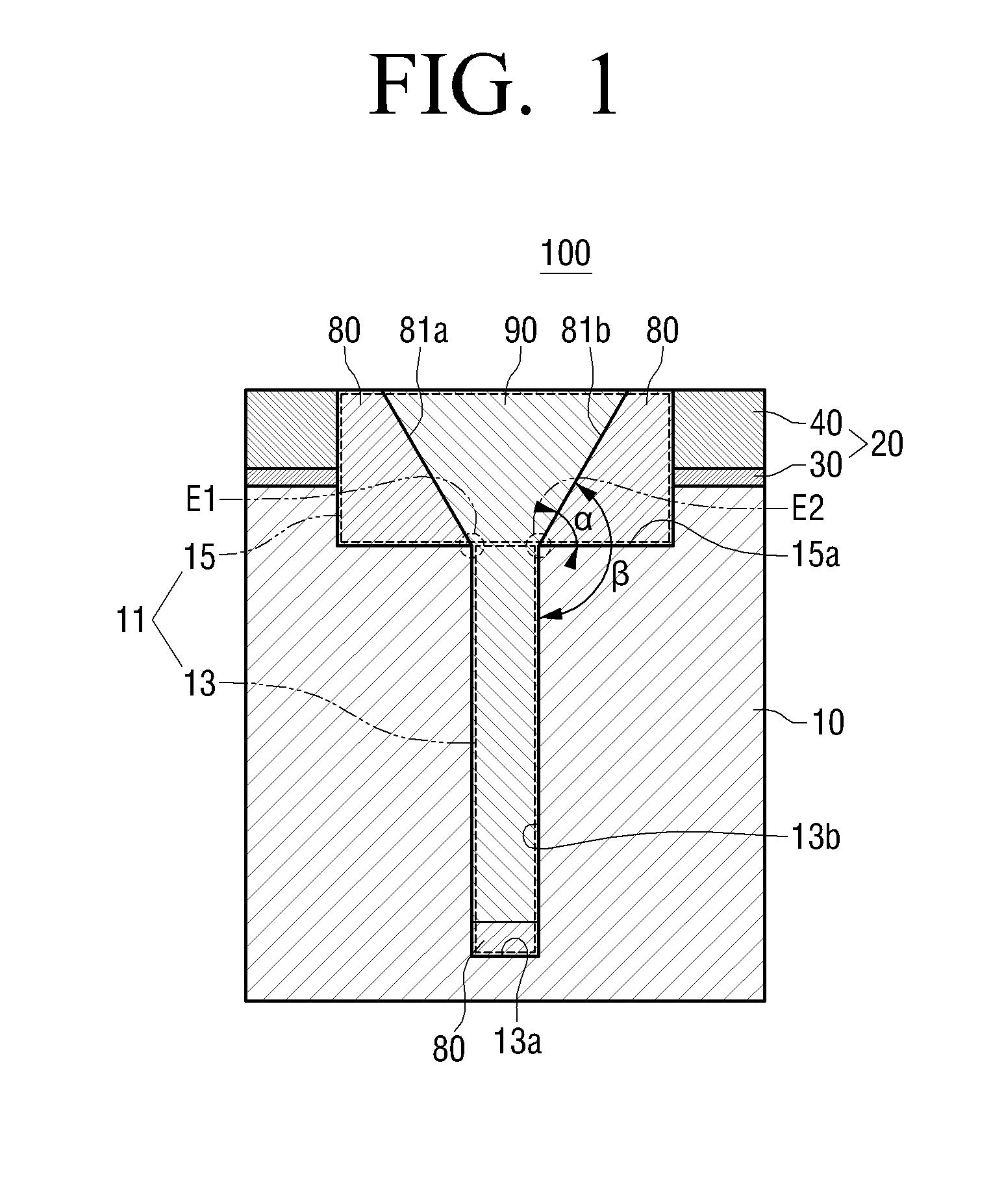
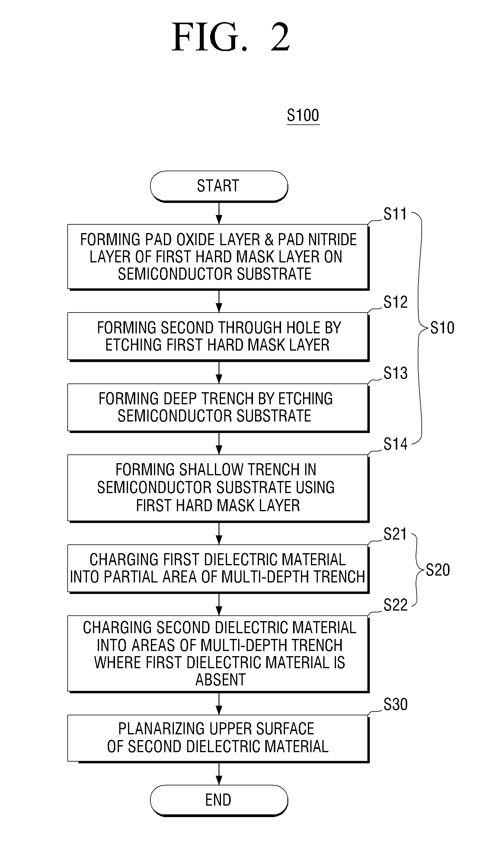
[0040]The following detailed description is provided to assist the reader in gaining a comprehensive understanding of the methods, apparatuses, and / or systems described herein. Accordingly, various changes, modifications, and equivalents of the systems, apparatuses and / or methods described herein will be suggested to those of ordinary skill in the art. The progression of processing steps and / or operations described is an example; however, the sequence of steps and / or operations is not limited to that set forth herein and may be changed as is known in the art, with the exception of steps and / or operations necessarily occurring in a certain order. Also, descriptions of well-known functions and constructions may be omitted for increased clarity and conciseness.

[0041]It is understood that the features of the present disclosure may be embodied in different forms and should not be constructed as limited to the examples set forth herein. Rather, examples are provided so that this disclosur...


PUM

PropertyMeasurementUnit
angleaaaaaaaaaa
angleaaaaaaaaaa
angleaaaaaaaaaa

Abstract

A semiconductor device and a method of fabricating the same are provided. The semiconductor device includes a semiconductor substrate in which a multi-depth trench is formed, the multi-depth trench including a shallow trench and a deep trench arranged below the shallow trench, a first dielectric material formed in partial area of the multi-depth trench, the first dielectric material including a slope in the shallow trench that extends upward from a corner where a bottom plane of the shallow trench and a sidewall of the deep trench meets, the slope being inclined with respect to the bottom plane of the shallow trench, and a second dielectric material formed in areas of the multi-depth trench in which the first dielectric material is absent.

Description

CROSS-REFERENCE TO RELATED APPLICATIONS[0001]This application claims the benefit under 35 U.S.C. §119(a) of Korean Patent Application No. 10-2010-0107704, filed on Nov. 1, 2010 and Korean Patent Application No. 10-2010-0122773, filed on Dec. 3, 2010, in the Korean Intellectual Property Office, the entire disclosure of which is incorporated herein by reference for all purposes.BACKGROUND[0002]1. Field[0003]The following description relates to a semiconductor device and a method of fabricating the same, and more particularly, to a semiconductor device in which a multi-depth trench with shallow trench depth and deep trench depth is formed in an element isolating region (inactive region) and a method for fabricating the same.[0004]2. Description of Related Art[0005]In general, trench isolation is one technique used to electrically separate active regions of a semiconductor device by forming trenches in an element isolating region (inactive region) and filling in dielectric material as a...

Claims


Application Information

Patent Timeline
Patent Type & Authority Applications(United States)
IPC IPC(8): H01L29/06H01L21/762
CPCH01L21/308H01L21/76232H01L21/76229H01L29/0649
Inventor WON, YONG-SIKLEE, SANG-UK
Owner KEY FOUNDRY CO LTD
Why Eureka
Try Eureka