
Three-dimensional coiling via structure for impedance tuning of impedance discontinuity

a three-dimensional coiling and discontinuity technology, applied in the field of substrate via technology, can solve the problems of signal distortion, signal power loss, signal insertion loss,

Active Publication Date: 2012-05-10
AVAGO TECH INT SALES PTE LTD
View PDF8 Cites 28 Cited by
  • Summary
  • Abstract
  • Description
  • Claims
  • Application Information

AI Technical Summary

Benefits of technology

[0011]Methods, systems, and apparatuses are described for three-dimensional coiling via structures substantially as shown in and / or described herein in connection with at least one of the figures, as set forth more completely in the claims.

Problems solved by technology

When the signal conducts through the conductor and encounters a subsequent conductor, the signal may be distorted in some manner.
As such, the mismatched impedances cause a distortion to the signal, which is undesired.
Insertion loss is the loss of signal power resulting from the presence of a discontinuity in a signal path.
If, however, the impedances of the features do not match, a portion of the signal will reflect from the point at which the mismatch occurs, and a portion of the signal will continue on in a distorted fashion.
This change in the impedance profile between the metal trace and the via and / or the BGA section is an impedance discontinuity that can cause significant deteriorating effects on insertion loss, return loss, and the signal quality on the receiver end.
However, the limits of this type of reduction may be reached before the desired target impedance is attained (i.e., the impedance does not increase enough to reach the desired value).
However, a problem with this technique is that the additional trace that is used degrades insertion loss (e.g., due to conductor, surface roughness, and dielectric losses) and occupies a significant amount of space and substrate real-estate.

Method used


Image

  • Three-dimensional coiling via structure for impedance tuning of impedance discontinuity
  • Three-dimensional coiling via structure for impedance tuning of impedance discontinuity
  • Three-dimensional coiling via structure for impedance tuning of impedance discontinuity

Examples


example embodiments

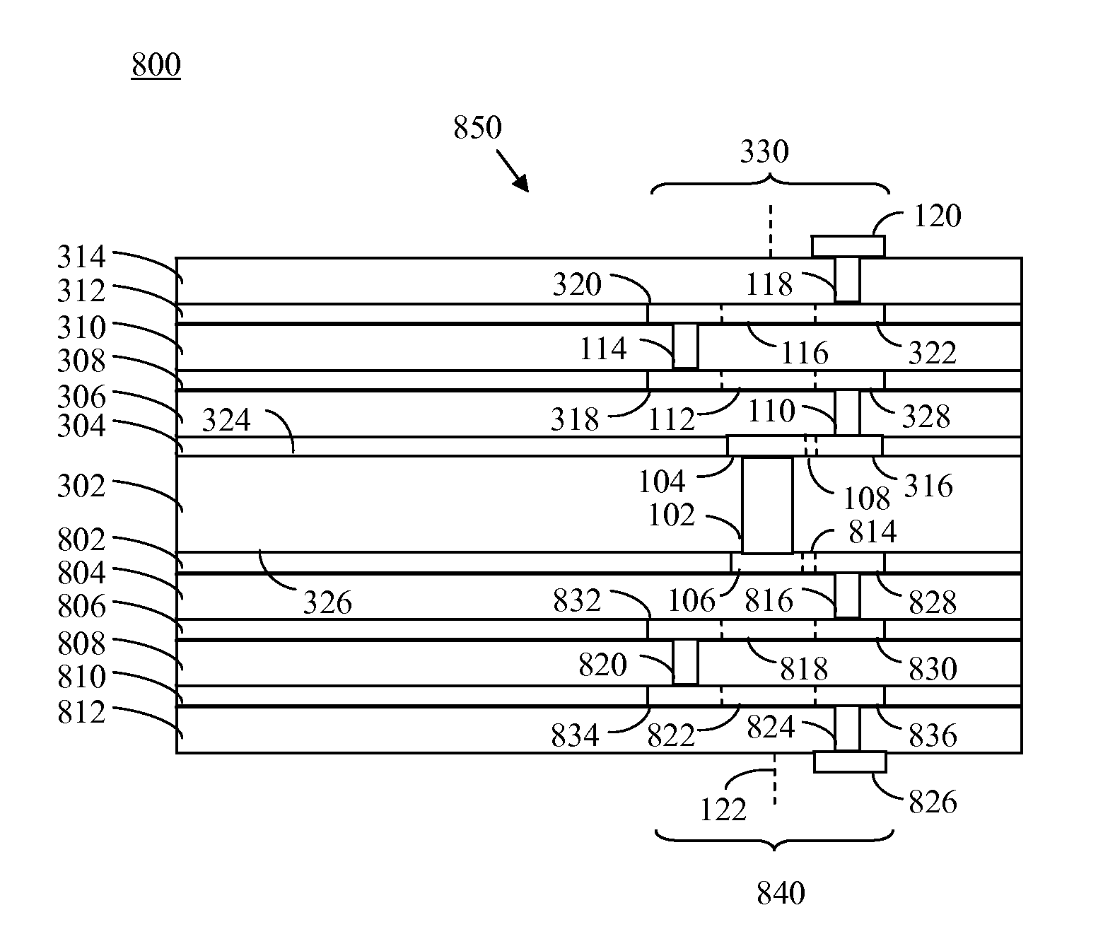
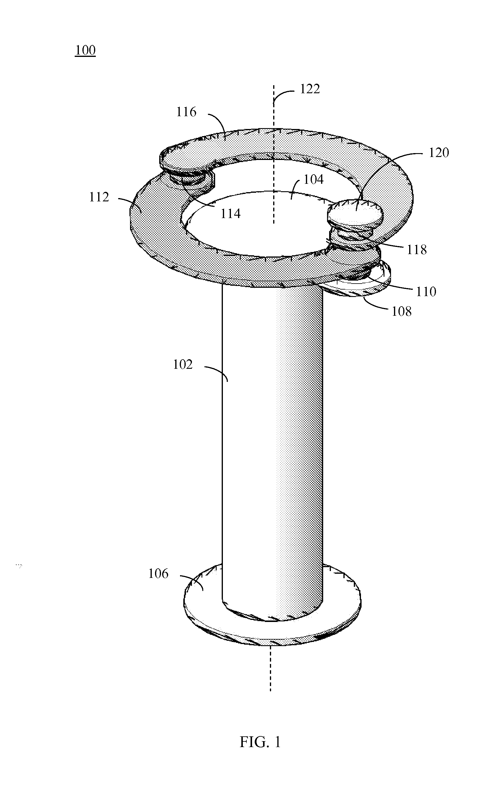
[0026]In embodiments, a three-dimensional (3D) coiling via structure or conductor is formed. The 3D coiling via structure may be used to tune signals transmitted through a substrate. For example, in an embodiment, a 3D coiling via structure may tune an impedance of a circuit discontinuity (e.g., via / BGA discontinuity) to match a trace impedance profile and to reduce / eliminate the discontinuity and reflections. The 3D coiling via structure may be tuned by adding or reducing partial or full coils or turns, and / or in further ways described elsewhere herein. The 3D coiling via structure / conductor may be implemented in various types of substrates, including circuit boards and substrates in integrated circuit (IC) packages. Examples of IC packages in which The 3D coiling via structure / conductor may be implemented include ball grid array (BGA) packages, quad flat packages (QFP), quad flat no lead (QFN) packages, land grid array (LGA) packages, pin grid array (PGA) packages, further types o...


PUM

PropertyMeasurementUnit
impedanceaaaaaaaaaa
impedanceaaaaaaaaaa
electrically conductiveaaaaaaaaaa

Abstract

Methods, systems, and apparatuses are provided for three-dimensional coiling via structures. A substrate includes a plurality of insulating layers, a plurality of trace layers interleaved with the insulating layers, and a three-dimensional coiling via. The three-dimensional coiling via includes a plurality of electrically conductive traces and a plurality of electrically conductive vias through the insulating layers. The electrically conductive traces are present in at least two of the traces layers and are coupled together by the electrically conductive vias. The electrically conductive traces are arranged to form at least one partial turn around an axis through the substrate.

Description

[0001]This application claims the benefit of U.S. Provisional Application No. 61 / 411,669, filed on Nov. 9, 2010, which is incorporated by reference herein in its entirety.BACKGROUND OF THE INVENTION[0002]1. Field of the Invention[0003]The present invention relates to substrate via technology.[0004]2. Background Art[0005]Electrical impedance, or simply impedance, describes a measure of opposition to alternating current (AC). When an AC signal is transmitted through a conductor, such as a metal trace, the conductor provides some resistance to the AC signal in the form of electrical impedance. The path of the signal may include further features beyond the conductor, such as further conductor including further traces, vias (electrical connections through layers of circuit boards), and other circuit elements or features that each have corresponding impedances. When the signal conducts through the conductor and encounters a subsequent conductor, the signal may be distorted in some manner....

Claims


Application Information

Patent Timeline
Patent Type & Authority Applications(United States)
IPC IPC(8): H01F5/04H05K3/00
CPCH05K1/0298H05K2203/041H01F5/003H05K1/0233H05K3/3436H05K1/165H01F41/041Y10T29/49124H01L2224/16227H01L2924/15311
Inventor SHARIFI, REZA
Owner AVAGO TECH INT SALES PTE LTD
Learn More