Automated Extraction of Size-Dependent Layout Parameters for Transistor Models

a transistor model and automatic extraction technology, applied in the simulation/interpretation/emulation of software, instruments, program control, etc., can solve the problems of not fully modeling the effect of modern strain engineering techniques, the effect of not being able to accurately incorporate the effects of transistor models, and the observation of tools affecting transistor performan

Inactive Publication Date: 2012-06-07
TEXAS INSTR INC
View PDF0 Cites 9 Cited by
  • Summary
  • Abstract
  • Description
  • Claims
  • Application Information

AI Technical Summary

Benefits of technology

[0022]FIG. 3a is a cross-sectional view of a MOS transistor illustrating

Problems solved by technology

In addition, the volume of strain-inducing material deployed at nearby active regions has also been observed to affect transistor performance.
These effects have not been accurately incorporated into transistor models, beyond the ability of some conventional modeling tools to identify the presence of nearby active regions to the modeled transistor, and in some cases the distance between the modeled transistor

Method used


Image

  • Automated Extraction of Size-Dependent Layout Parameters for Transistor Models
  • Automated Extraction of Size-Dependent Layout Parameters for Transistor Models
  • Automated Extraction of Size-Dependent Layout Parameters for Transistor Models

Examples


Embodiment Construction

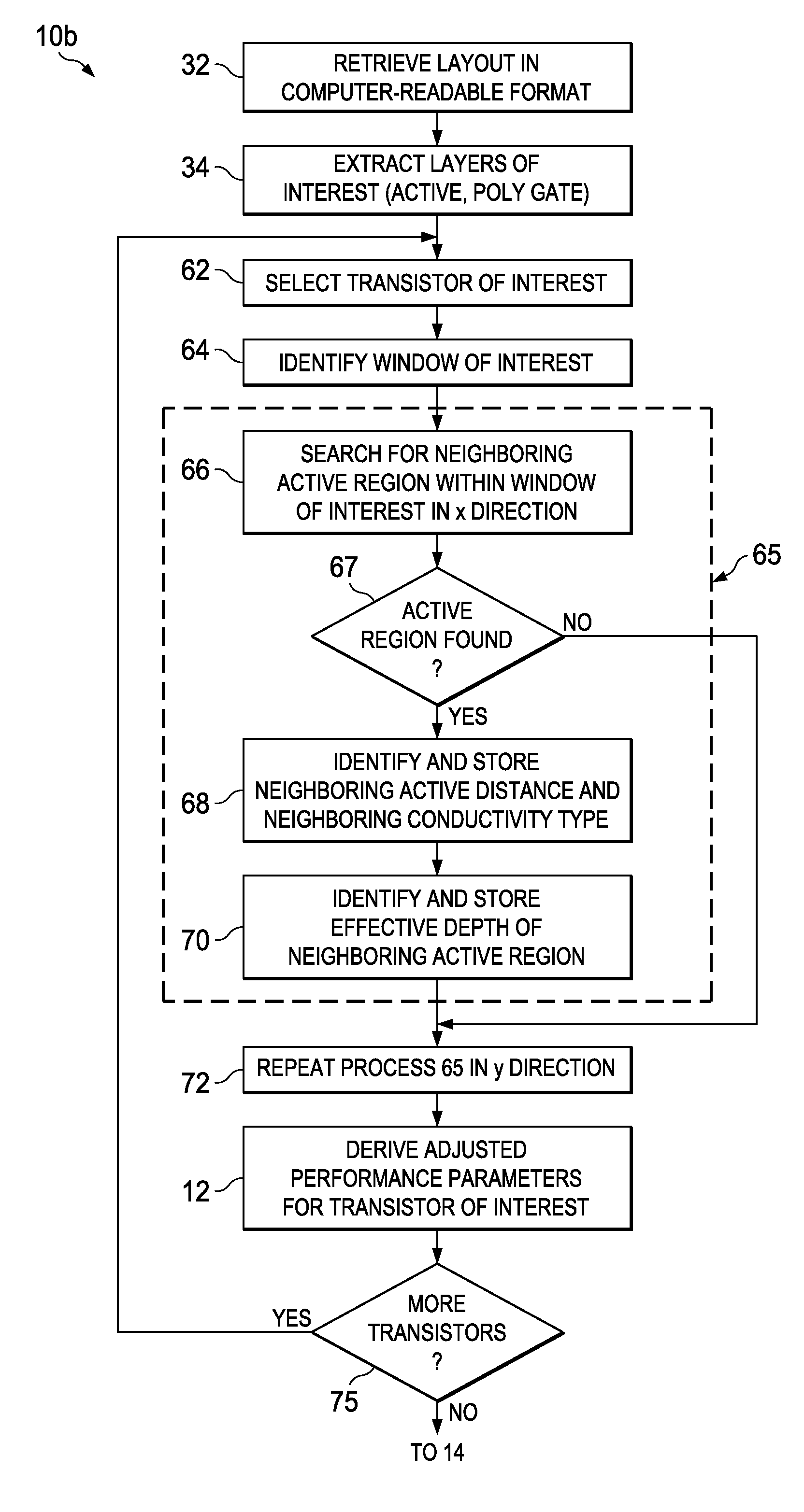
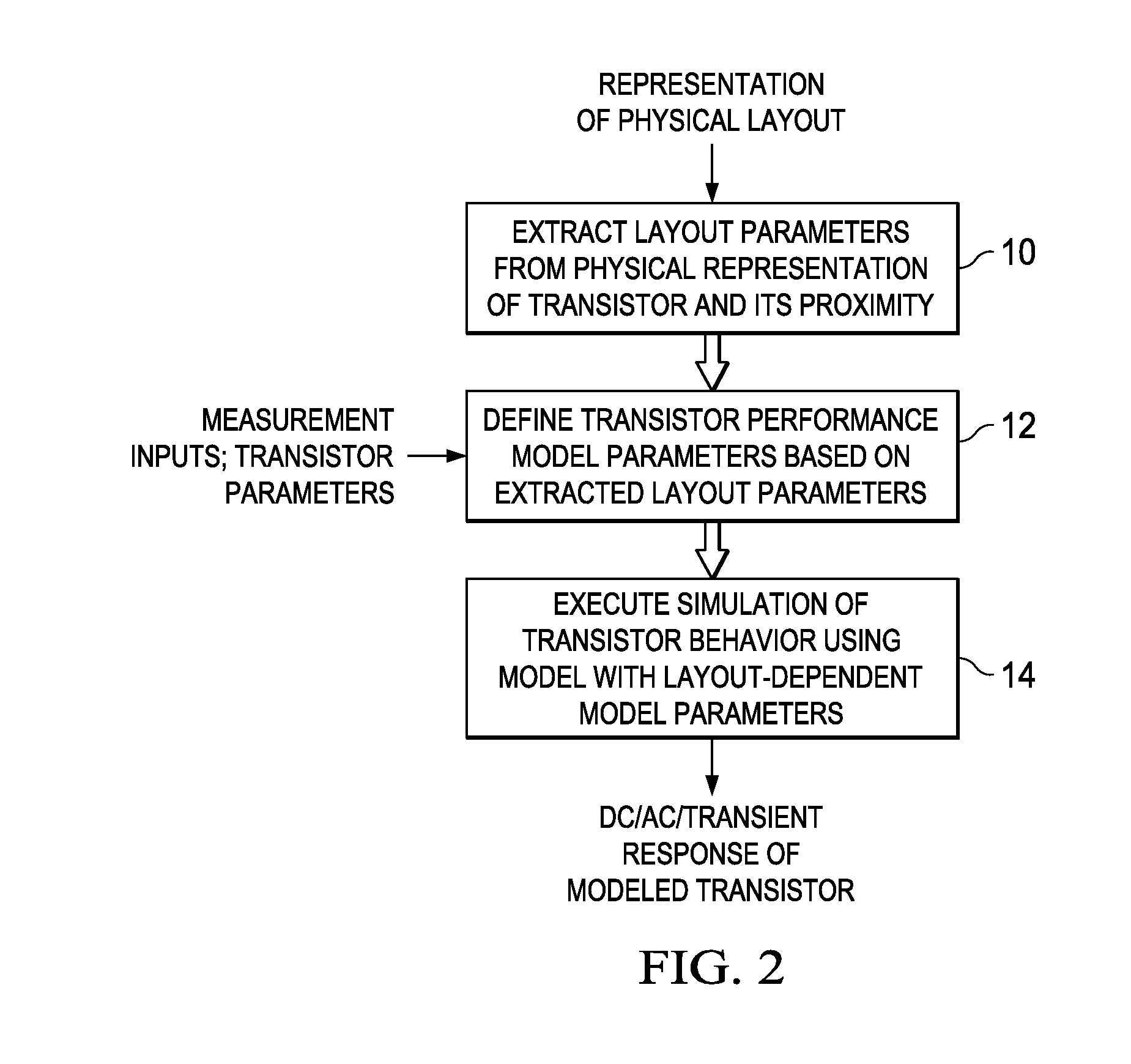
[0029]This invention will be described in connection with one or more of its embodiments, namely as implemented into a computer system programmed to model the performance of metal-oxide-semiconductor (MOS) transistors for the effects of layout parameters, as it is contemplated that this invention will be especially beneficial when applied in such a manner. However, it is contemplated that the layout extraction performed according to this invention will be beneficial in modeling a wide range of integrated circuit devices for various effects other than those described herein. Accordingly, it is to be understood that the following description is provided by way of example only, and is not intended to limit the true scope of this invention as claimed.

[0030]Modeling and Simulation System

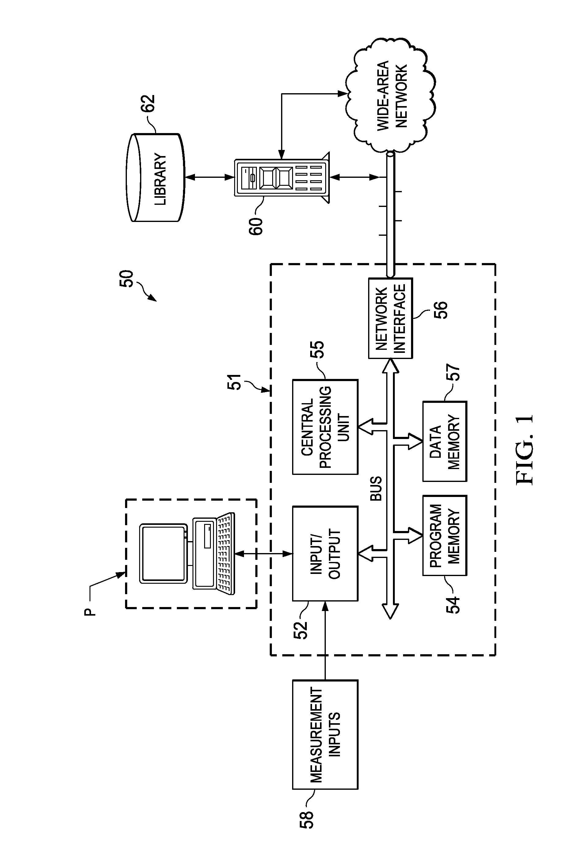
[0031]Referring to FIG. 1, computing system 50 for deriving and storing a transistor model generated according to embodiments of this invention, and for applying that model in the simulation of an electro...


PUM


Abstract

A system and method for determining transistor model parameters that account for layout-dependent features in the transistor being modeled, and also in neighboring devices in the same integrated circuit. A computer-readable expression of the integrated circuit layout is retrieved, and active and gate layers in that expression extracted. For a transistor being modeled, its active regions are analyzed to determine whether these regions have a complex shape. Model parameters are derived based on volume effects of the complex shaped active regions. Neighboring active regions that affect parameters of the transistor being modeled are also identified and their effective depth determined. Strain effects due to complex shaped active regions and neighboring elements are thus included in the transistor model.

Description

CROSS-REFERENCE TO RELATED APPLICATIONS[0001]Not applicable.STATEMENT REGARDING FEDERALLY SPONSORED RESEARCH OR DEVELOPMENT[0002]Not applicable.BACKGROUND OF THE INVENTION[0003]This invention is in the field of simulation of integrated circuits, and is more specifically directed to the modeling of metal-oxide-semiconductor (MOS) transistor performance including the effects of structure layout, as applied to such simulation.[0004]Simulation of the operation of electronic circuits is a staple task in the design of integrated circuits, even for the most simple of functions but especially as integrated circuit functionality and complexity have increased over time. Modern circuit simulation tools not only allow the circuit designer to verify that a circuit carries out its intended function, but also enable the designer to evaluate the robustness of circuit operation over variations in temperature, signal levels, power supply voltages, and process parameters. A well-known circuit simulati...

Claims


Application Information

Patent Timeline
IPC IPC(8): G06F17/50G06F9/455
CPCG06F17/5036G06F30/367
Inventor OLUBUYIDE, OLUWAMUYIWA OLUWAGBEMIGAKOLARIK, DONALD MARK
Owner TEXAS INSTR INC
Why Eureka
Try Eureka