

Page buffer circuit
a buffer circuit and buffer technology, applied in the field of semiconductor memory apparatus, can solve the problems of disadvantageous integration of semiconductor apparatus, error may occur in the storage latch value,
- Summary
- Abstract
- Description
- Claims
- Application Information
AI Technical Summary
Benefits of technology
Problems solved by technology
Method used
Image

Examples
Embodiment Construction
[0031]Reference will now be made in detail to the exemplary embodiments consistent with the present disclosure, examples of which are illustrated in the accompanying drawings. Wherever possible, the same reference characters will be used throughout the drawings to refer to the same or like parts.
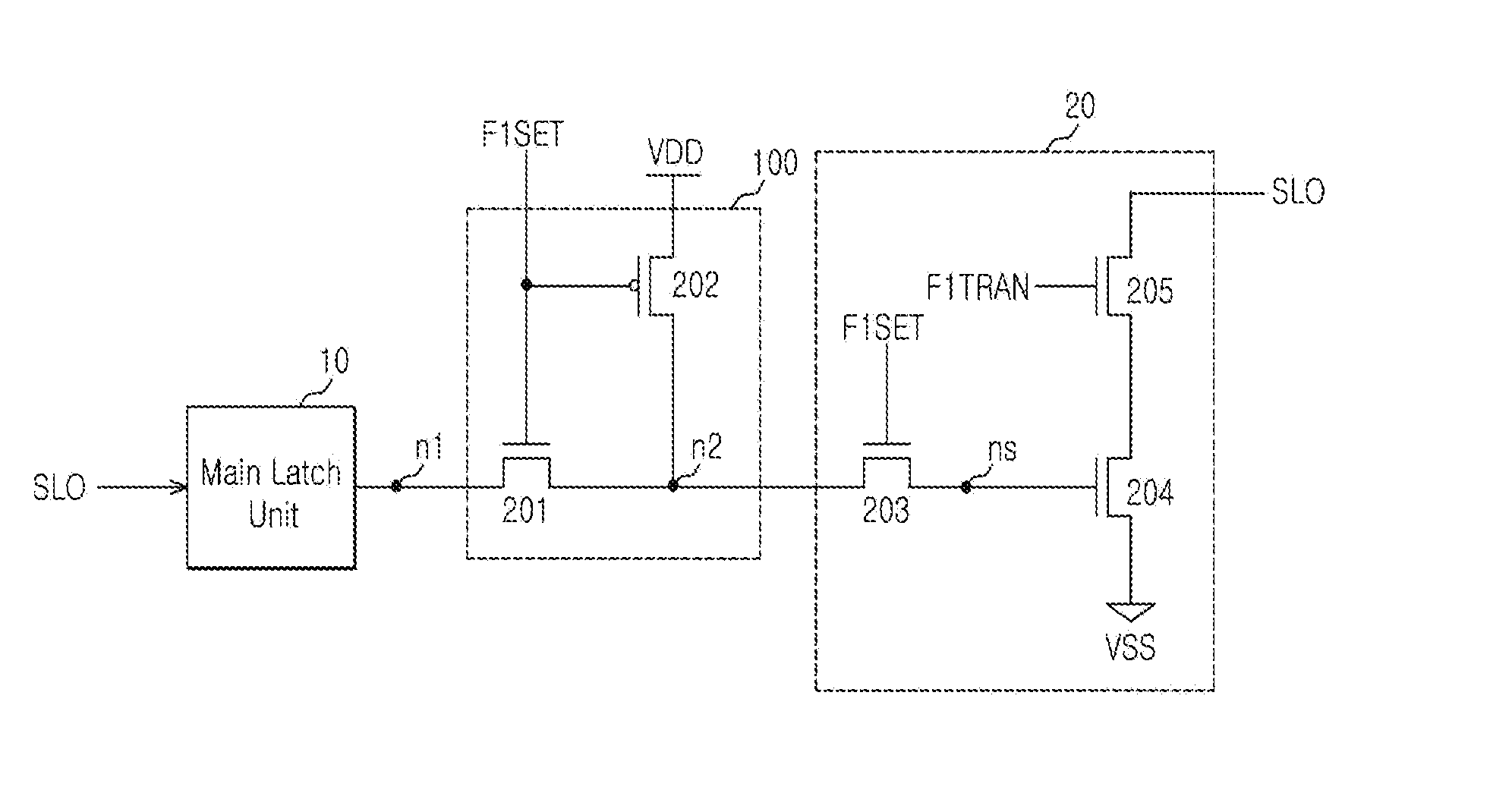
[0032]FIG. 2 is a circuit diagram of a page buffer circuit according to one exemplary embodiment.
[0033]The page buffer circuit may include a main latch unit 10, a sub latch unit 20, and a voltage determination unit 100.
[0034]The main latch unit 10 may have a main latch value which is dependent on a sub latch output signal SLO, and outputs the main latch value to a first node n1.
[0035]The sub latch unit 20 latches a voltage of a second node n2 as a sub latch value in response to a storage enable signal F1SET, and generates the sub latch output signal SLO according to the sub latch value when an output enable signal F1TRAN is activated.
[0036]The voltage determination unit 100 may be connected ...
PUM
 Abstract
Description
Claims
Application Information