Electronic component and substrate module
a technology applied in the field of electronic components and substrate modules, can solve problems such as the risk of short circuits, and achieve the effects of preventing short circuits, suppressing short circuits, and reducing esl
- Summary
- Abstract
- Description
- Claims
- Application Information
AI Technical Summary
Benefits of technology
Problems solved by technology
Method used
Image

Examples
first preferred embodiment
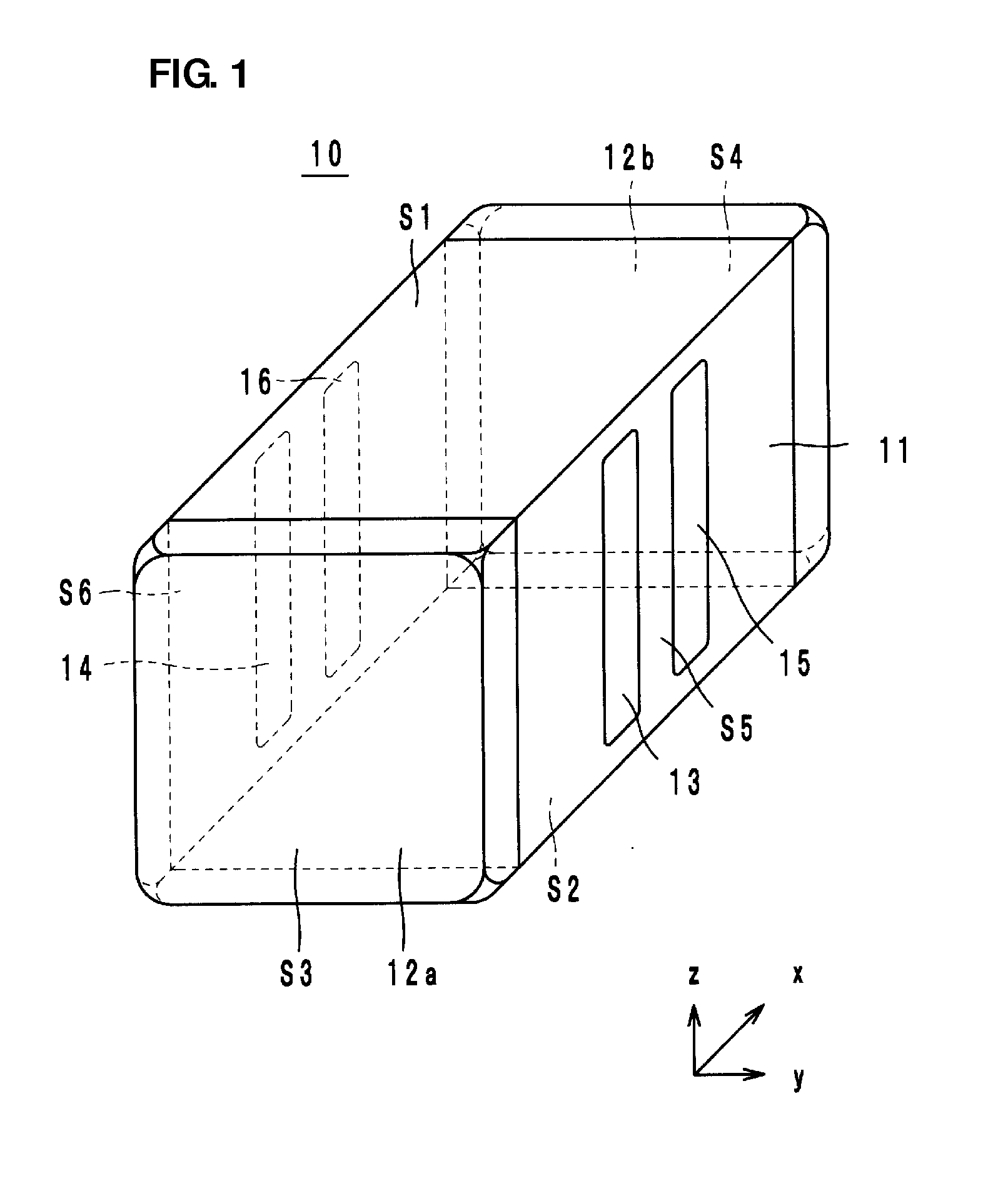
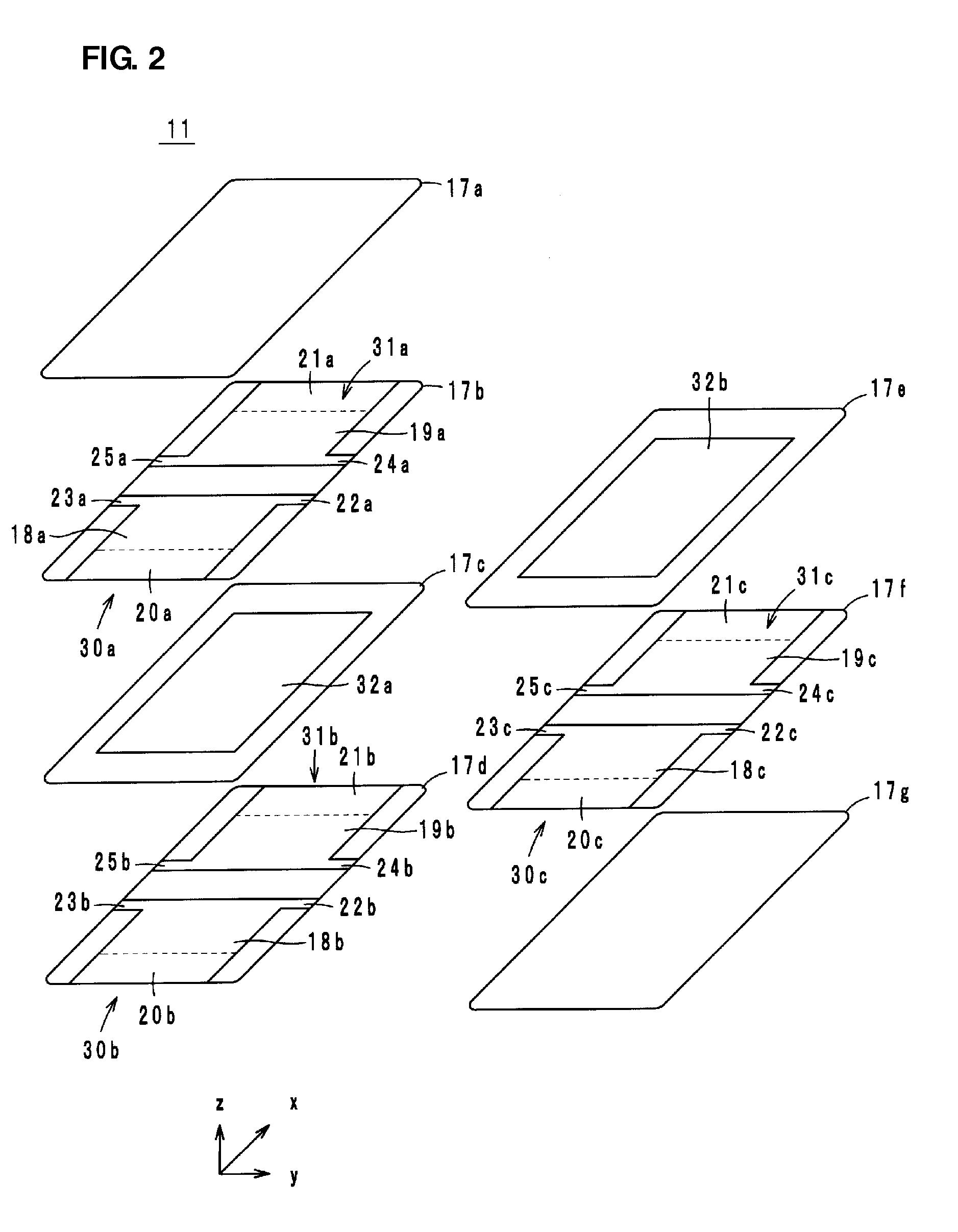
[0035]First, the configuration of an electronic component according to a first preferred embodiment will be described with reference to the drawings. FIG. 1 is an external perspective view of an electronic component 10 according to the first preferred embodiment. FIG. 2 is an exploded perspective view of a multilayer body 11 of the electronic component 10 of FIG. 1. FIGS. 3A and 3B are plan views of the inside of the electronic component 10 of FIG. 1. Hereafter, a stacking direction of the multilayer body 11 will be defined as a z-axis direction. A direction in which the long sides of the multilayer body 11 extend when the multilayer body 11 is viewed in plan from the z-axis direction will be defined as an x-axis direction. A direction in which the short sides of the multilayer body 11 extend when the multilayer body 11 is viewed in plan from the z-axis direction will be defined as a y-axis direction.
[0036]The electronic component 10 is, for example, a chip capacitor and, as illustr...
second preferred embodiment
[0099]Hereafter, an electronic component and a substrate module according to a second preferred embodiment will be described with reference to the drawings. FIG. 12 is an external perspective view of an electronic component 10a according to the second preferred embodiment.
[0100]In the electronic component 10a, the external electrodes 13 and 15 are folded over from the side surface S5 onto the upper surface S1 and the lower surface S2. In addition, the external electrodes 14 and 16 are folded over from the side surface S6 onto the upper surface S1 and the lower surface S2. Other aspects of the configuration of the electronic component 10a are the same as those of the electronic component 10 and therefore description thereof will be omitted.
[0101]With the above-described electronic component 10a, similarly to as with the electronic component 10, a significant reduction in ESL can be achieved and the occurrence of short circuits when mounting the electronic component 10a on a circuit s...
first modification
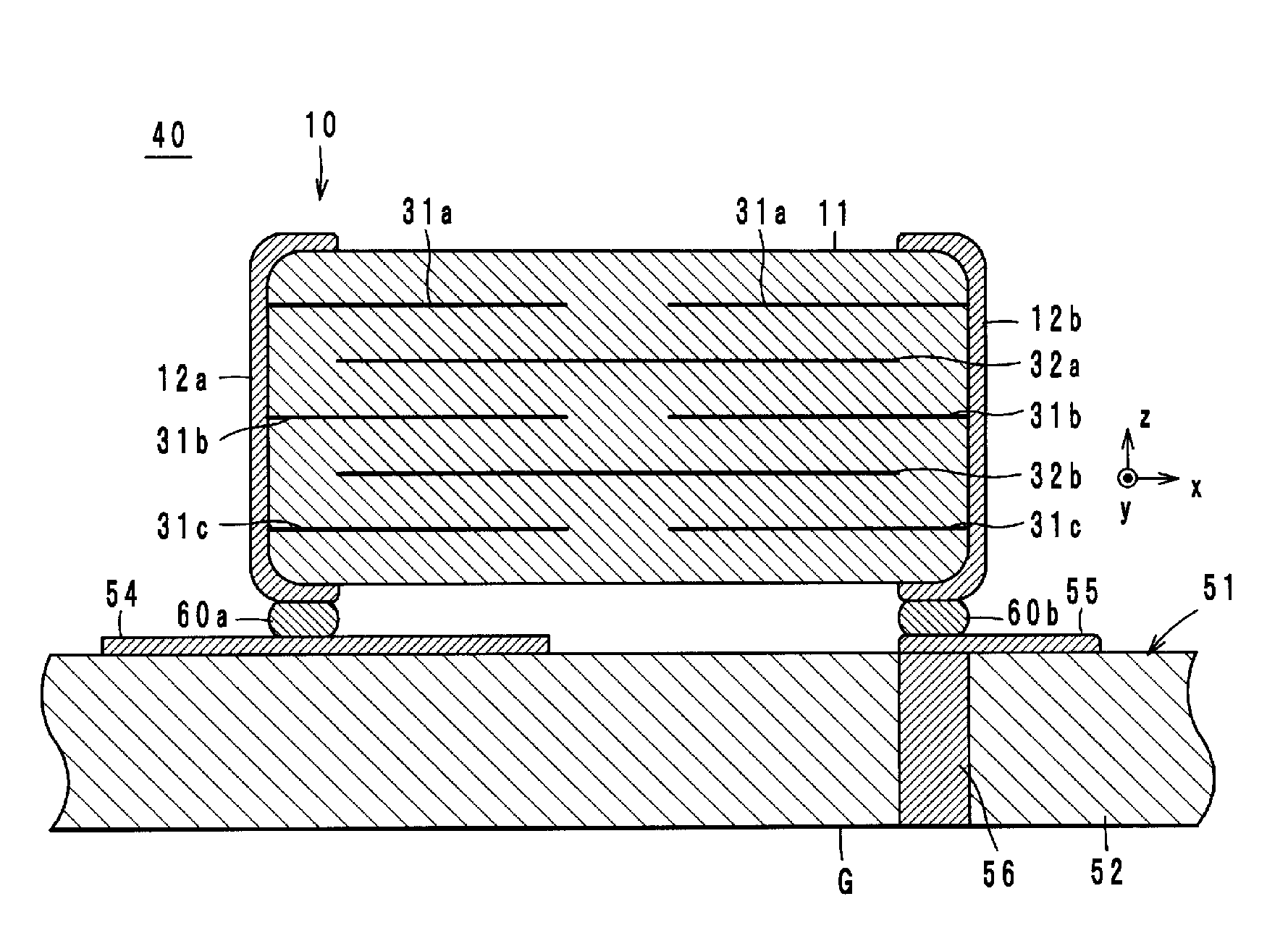
[0104]Next, a substrate module according to a first modification will be described with reference to the drawings. FIG. 14 is a sectional structural view of a substrate module 40b.
[0105]The substrate module 40b differs from the substrate module 40a in that the external electrodes 15 and 16 are connected to the ground electrode 55 with solder 60c. Since there are no other differences, description of other aspects of the configuration of the substrate module 40b will be omitted.
[0106]In the substrate module 40a, a high-frequency signal passes along the first path and the second path. On the other hand, in the substrate module 40b, a high-frequency signal passes along a third path and a fourth path to be described below, as well as along the first path and the second path.
[0107]The third path is a path in which a high-frequency signal flows through the signal conductor 54, the external electrode 12a, the led out conductor 20, the capacitance conductor 18, the internal conductor 32, th...
PUM
 Abstract
Description
Claims
Application Information
 - R&D
- Intellectual Property
- Life Sciences
- Materials
- Tech Scout
- Unparalleled Data Quality
- Higher Quality Content
- 60% Fewer Hallucinations
Browse by: Latest US Patents, China's latest patents, Technical Efficacy Thesaurus, Application Domain, Technology Topic, Popular Technical Reports.
© 2025 PatSnap. All rights reserved.Legal|Privacy policy|Modern Slavery Act Transparency Statement|Sitemap|About US| Contact US: help@patsnap.com