Tandem solar cell with improved absorption material

a solar cell and absorption material technology, applied in the field of solar cells, can solve the problems of high cost, slow growth rate of cells during manufacture, and excessive current sharing between the top and bottom cells

Inactive Publication Date: 2012-09-06
IBM CORP
View PDF12 Cites 9 Cited by
  • Summary
  • Abstract
  • Description
  • Claims
  • Application Information

AI Technical Summary

Problems solved by technology

These types of cells suffer from slow growth rates during manufacture.
This results in higher cost.
In addition, since a top cell in such device also includes a form of Silicon, current sharing between the top and bottom cells is excessive, e.g., Jsc for the tandem device is often less than Jsc for an individual cell.
Thin-film materials of the type Cu(In,Ga)(S,Se)2 (CIGS), while efficient, include rare i

Method used


Image

  • Tandem solar cell with improved absorption material
  • Tandem solar cell with improved absorption material
  • Tandem solar cell with improved absorption material

Examples


Embodiment Construction

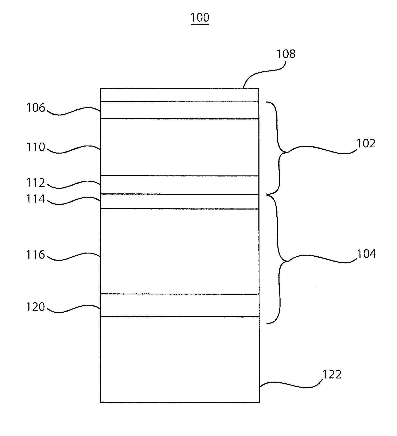
[0019]In accordance with the present principles, a new tandem solar cell device structure is provided that increases productivity and performance over conventional cells which typically employ microcrystalline silicon bottom cells. Greater efficiency is provided at least in part by less current sharing between top and bottom cells in the tandem structure. Further, the present embodiments provide tandem cells composed of materials which are rapidly grown or applied with high quality. This makes the present embodiments more cost effective in addition to other advantages.

[0020]In one illustrative embodiment, a tandem cell is fabricated having a one cell fabricated using a Cu—Zn—Sn containing chalcogenide compound with a kesterite structure of the formula: Cu2-xZn1+ySn(S1-zSez)4+q wherein 0≦x≦1; 0≦y≦1; 0≦z≦1; −1≦q≦1. In a particularly useful embodiment, Cu2ZnSn(S, Se)4 (CZTS or CZTSe) is employed. CZTS has many benefits. It is low cost and environmentally harmless being fabricated using...


PUM

PropertyMeasurementUnit
Fractionaaaaaaaaaa
Efficiencyaaaaaaaaaa
Band gapaaaaaaaaaa

Abstract

A photosensitive device and method includes a top cell having an N-type layer, a P-type layer and a top intrinsic layer therebetween. A bottom cell includes an N-type layer, a P-type layer and a bottom intrinsic layer therebetween. The bottom intrinsic layer includes a Cu—Zn—Sn containing chalcogenide.

Description

BACKGROUND[0001]1. Technical Field[0002]The present invention relates to solar cells and more particularly to a tandem solar cell device and method to achieve greater collection efficiency.[0003]2. Description of the Related Art[0004]Solar cells employ photovoltaic cells to generate current flow. Photons in sunlight hit a solar cell or panel and are absorbed by semiconducting materials, such as silicon. Electrons gain energy allowing them to flow through the material to produce electricity.[0005]When a photon hits silicon, the photon may be transmitted through the silicon, the photon can reflect off the surface, or the photon can be absorbed by the silicon, if the photon energy is higher than the silicon band gap value. This generates an electron-hole pair and sometimes heat, depending on the band structure. When a photon is absorbed, its energy is given to an electron in a crystal lattice. Electrons in the valence band may be excited into the conduction band, where they are free to...

Claims


Application Information

Patent Timeline
IPC IPC(8): H01L31/06H01L31/18
CPCH01L31/18Y02E10/548H01L31/078H01L31/076Y02E10/541C23C14/34H01L31/0326H01L31/20
Inventor GUNAWAN, OKIKIM, JEEHWANMITZI, DAVID B.SADANA, DEVENDRA K.TODOROV, TEODOR K.
Owner IBM CORP
Why Eureka
Try Eureka