Planar light source device, liquid crystal display device, and television set

US20120224111A1Inactive Publication Date: 2012-09-06PANASONIC LIQUID CRYSTAL DISPLAY CO LTD

Image

  • Planar light source device, liquid crystal display device, and television set
  • Planar light source device, liquid crystal display device, and television set
  • Planar light source device, liquid crystal display device, and television set

Examples


Embodiment Construction

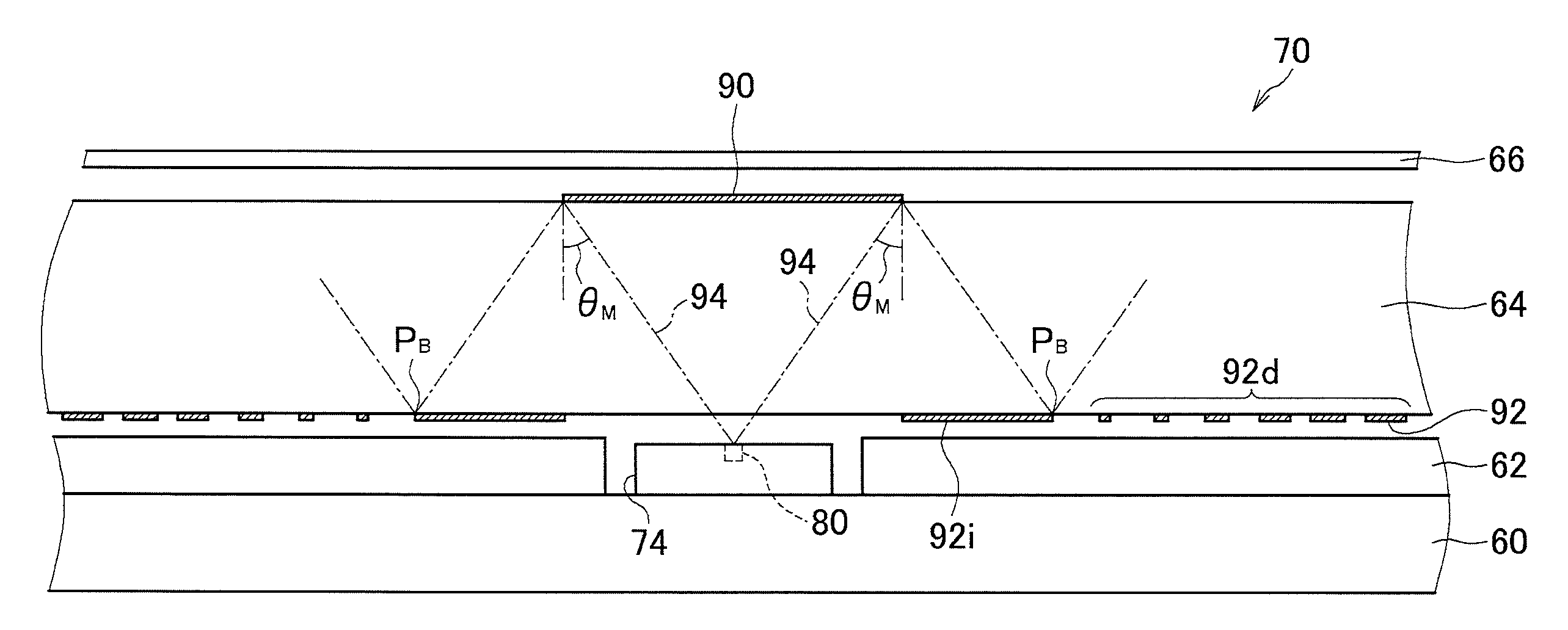
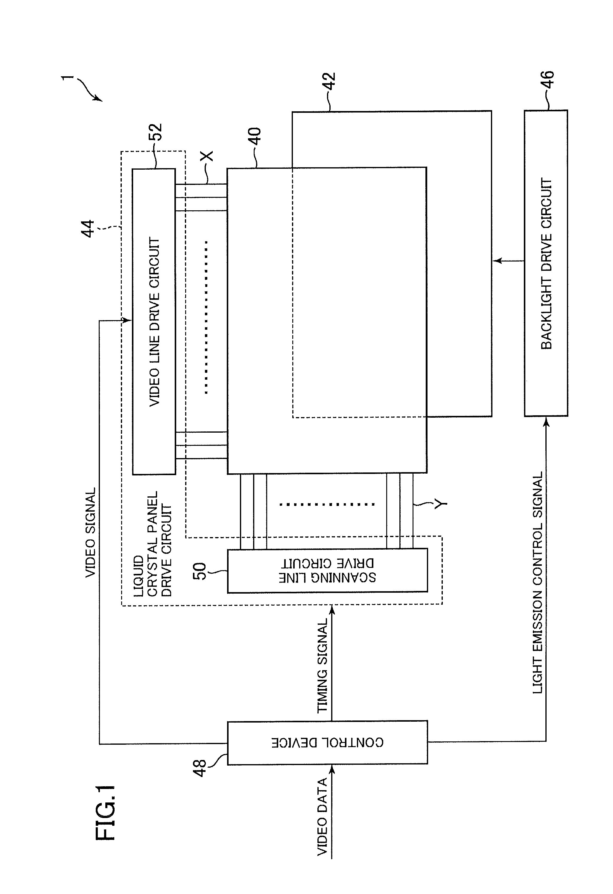
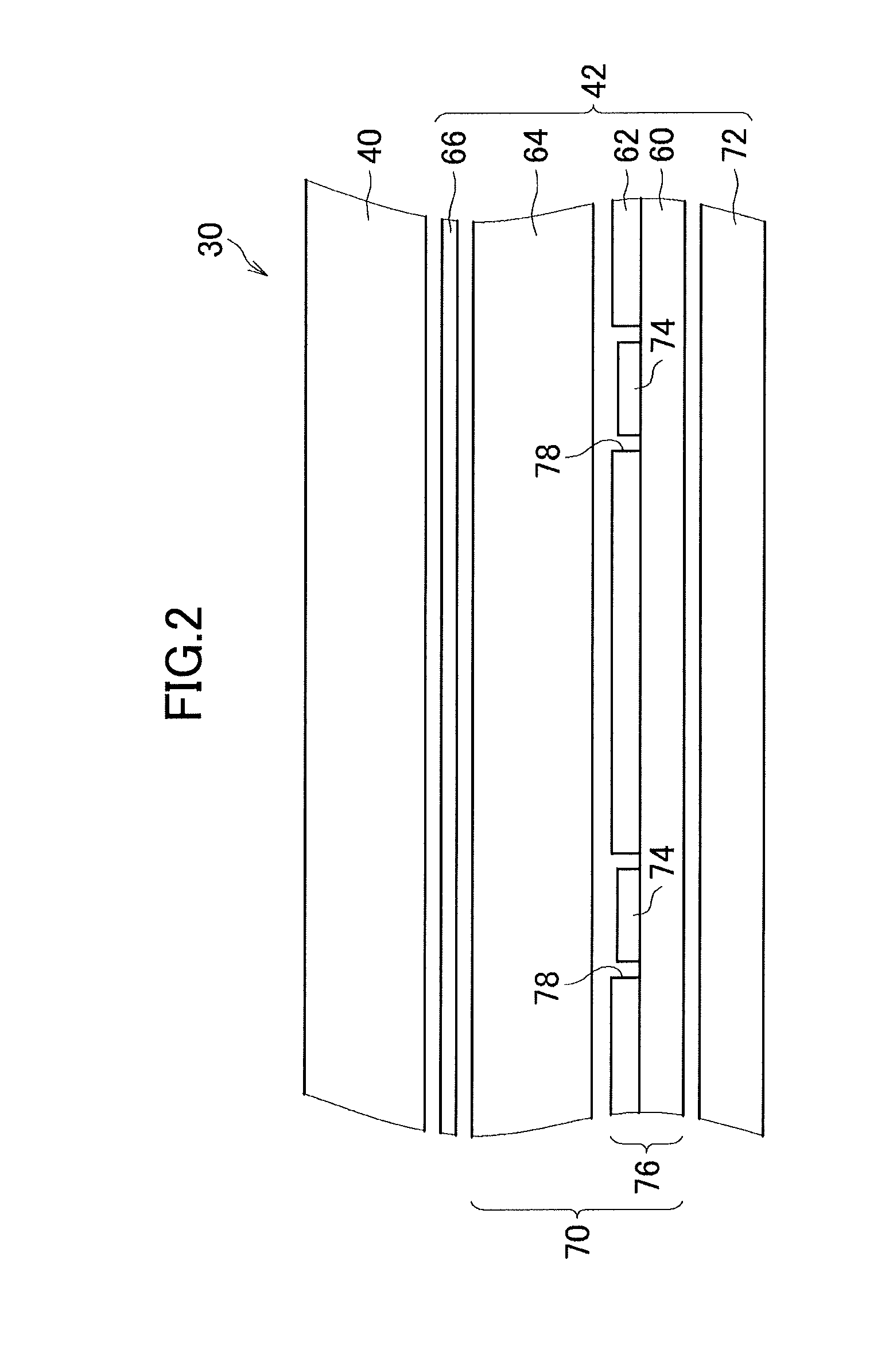
[0035]Hereinafter, an embodiment of the present invention is described with reference to the accompanying drawings. FIG. 1 is a schematic diagram illustrating a configuration of a liquid crystal display device 30 according to the embodiment of the present invention.

[0036]As illustrated in FIG. 1, the liquid crystal display device 30 includes a liquid crystal panel 40, a backlight unit 42, a liquid crystal panel drive circuit 44, a backlight drive circuit 46, and a control device 48. The liquid crystal panel drive circuit 44 includes a scanning line drive circuit 50 and a video line drive circuit 52.

[0037]The liquid crystal panel 40 is a laminate including a pair of transparent glass substrates, liquid crystal sandwiched therebetween, and polarizing plates respectively adhered to a display surface-side surface of one of the pair of glass substrates sandwiching the liquid crystal and a backlight unit-side surface of the other glass substrate. The liquid crystal panel 40 has a substant...


PUM


Abstract

In a direct type backlight device of a liquid crystal display device, a light guide plate is used obtain a uniform in-plane distribution of light emission intensity. A reflective sheet (62) having an opening portion is laminated on a front surface of an LED substrate (60), and an LED element (74) is accommodated inside the opening portion. A light guide plate (64) is stacked on the reflective sheet (62). On a front surface of the light guide plate (64), a white reflective film (90) is formed in a non-total reflection region, which is positioned to oppose the LED element (74) and in which an incident angle of light emitted from the LED element (74) to the front surface is smaller than a critical angle. On a rear surface of the light guide plate (64), a pattern made of a white reflective film (92) is formed.

Description

CROSS-REFERENCE TO RELATED APPLICATION[0001]The present application claims priority from Japanese application JP 2011-044398 filed on Mar. 1, 2011, the content of which is hereby incorporated by reference into this application.BACKGROUND OF THE INVENTION[0002]1. Field of the Invention[0003]The present invention relates to a planar light source device, a liquid crystal display device, and a television set, and more particularly, to a technology of using a light guide plate to obtain planar light emission from a non-planar light source such as a light emitting diode (LED).[0004]2. Description of the Related Art[0005]Liquid crystal display devices are used for personal computer displays, liquid crystal television sets, and the like. In the liquid crystal display device, each pixel of a liquid crystal panel for forming an image does not emit light by itself. Accordingly, the liquid crystal display device includes a light source for irradiating the liquid crystal panel with light, and th...

Claims


Application Information

Patent Timeline
06 Sep 2012
Publication
US20120224111A1
IPC
H04N3/10; G02F1/13357; F21V8/00
CPC
G02F1/133603; G02F1/133611; G02F1/133606
Inventors
OHSHIMA, YOSHINORI