Memory device and method of controlling a write operation within a memory device

a memory device and write operation technology, applied in the field of memory devices, can solve the problems of reducing the possibility that non-addressed memory cells could become corrupted, and achieve the effect of simple and effective techniqu

Active Publication Date: 2012-09-13
ARM LTD
View PDF3 Cites 12 Cited by
  • Summary
  • Abstract
  • Description
  • Claims
  • Application Information

AI Technical Summary

Benefits of technology

[0020]In one particular embodiment, the signal line is precharged to a logic one level, and each comparison block is arranged to discharge the voltage on the signal line if a match is not detected between the data bit currently stored in the associated addressed memory cell and the corresponding bit of the data word forming the write data. Accordingly, it will be understood that during each iteration of the comparison operation, the signal line will be discharged unless all of the addressed memory cells have correctly stored the associated bit of the write data. The comparison operation is then repeated until the evaluation block observes that the voltage on the signal line has not been altered during the operation of the comparison blocks, at which point the control signal is asserted. This provides a particularly simple and effective technique for implementing the required functions of the comparing circuitry.

Problems solved by technology

In addition, the ability to keep the pulse width as short as possible having regards to the actual addressed memory cells reduces the earlier-mentioned half select problem, since in designs of memory device where other non-addressed memory cells may also be subjected to the asserted write word line signal, the fact that the write word line signal is only asserted for as long as necessary to ensure that the write data is written also reduces the prospect that those non-addressed memory cells could become corrupted.

Method used


Image

  • Memory device and method of controlling a write operation within a memory device
  • Memory device and method of controlling a write operation within a memory device
  • Memory device and method of controlling a write operation within a memory device

Examples


Embodiment Construction

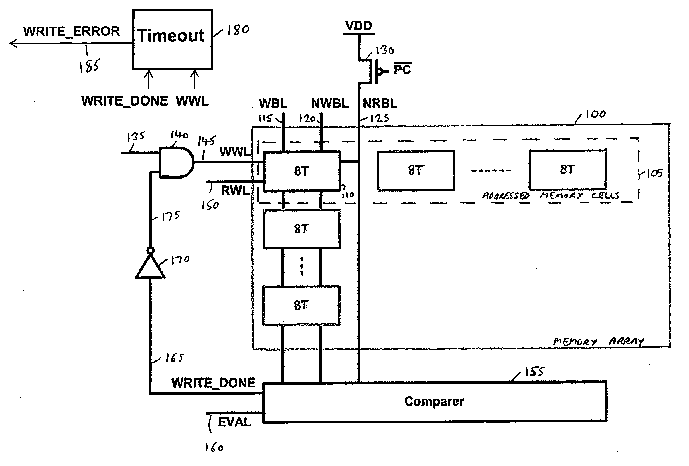
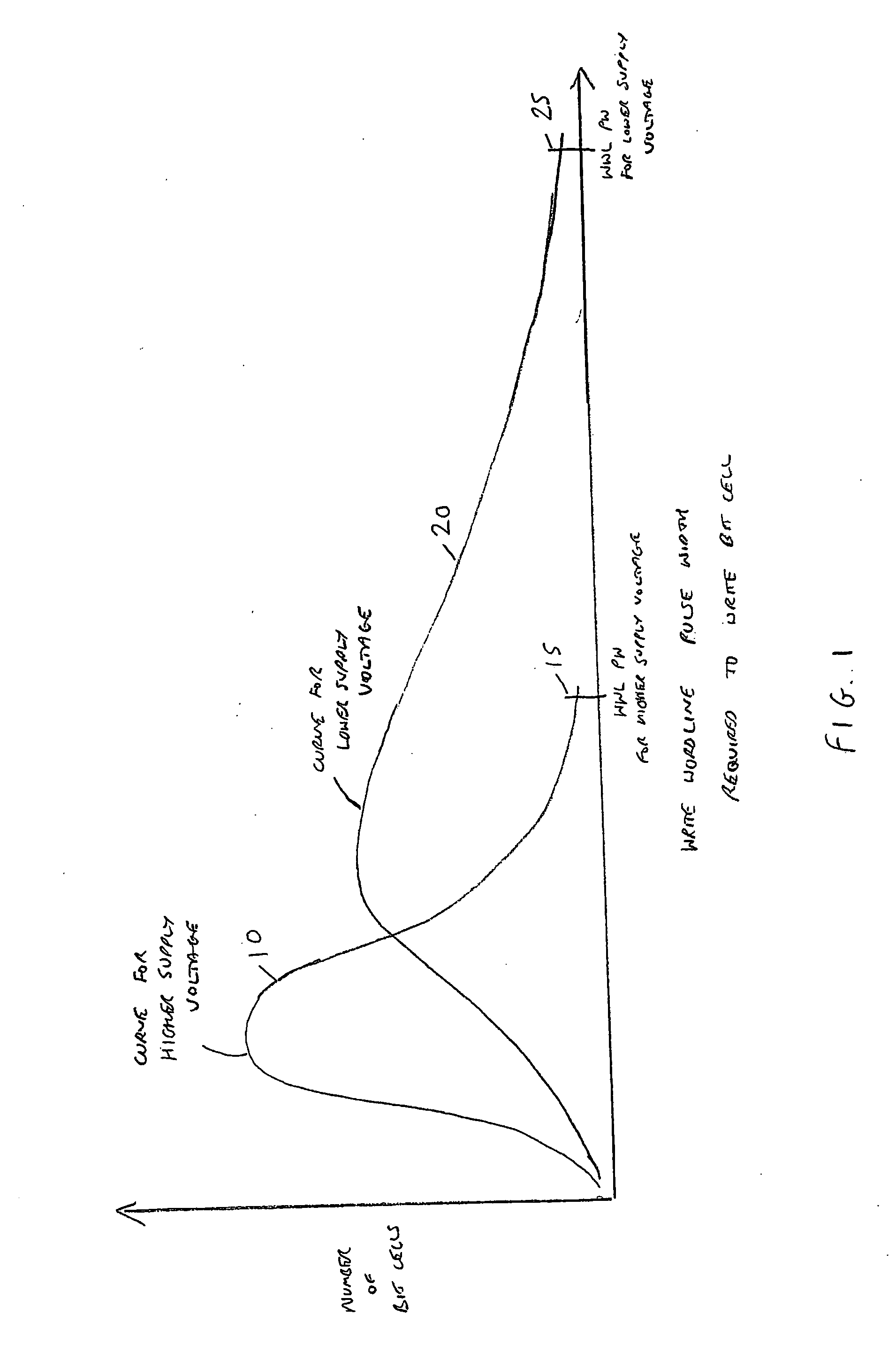
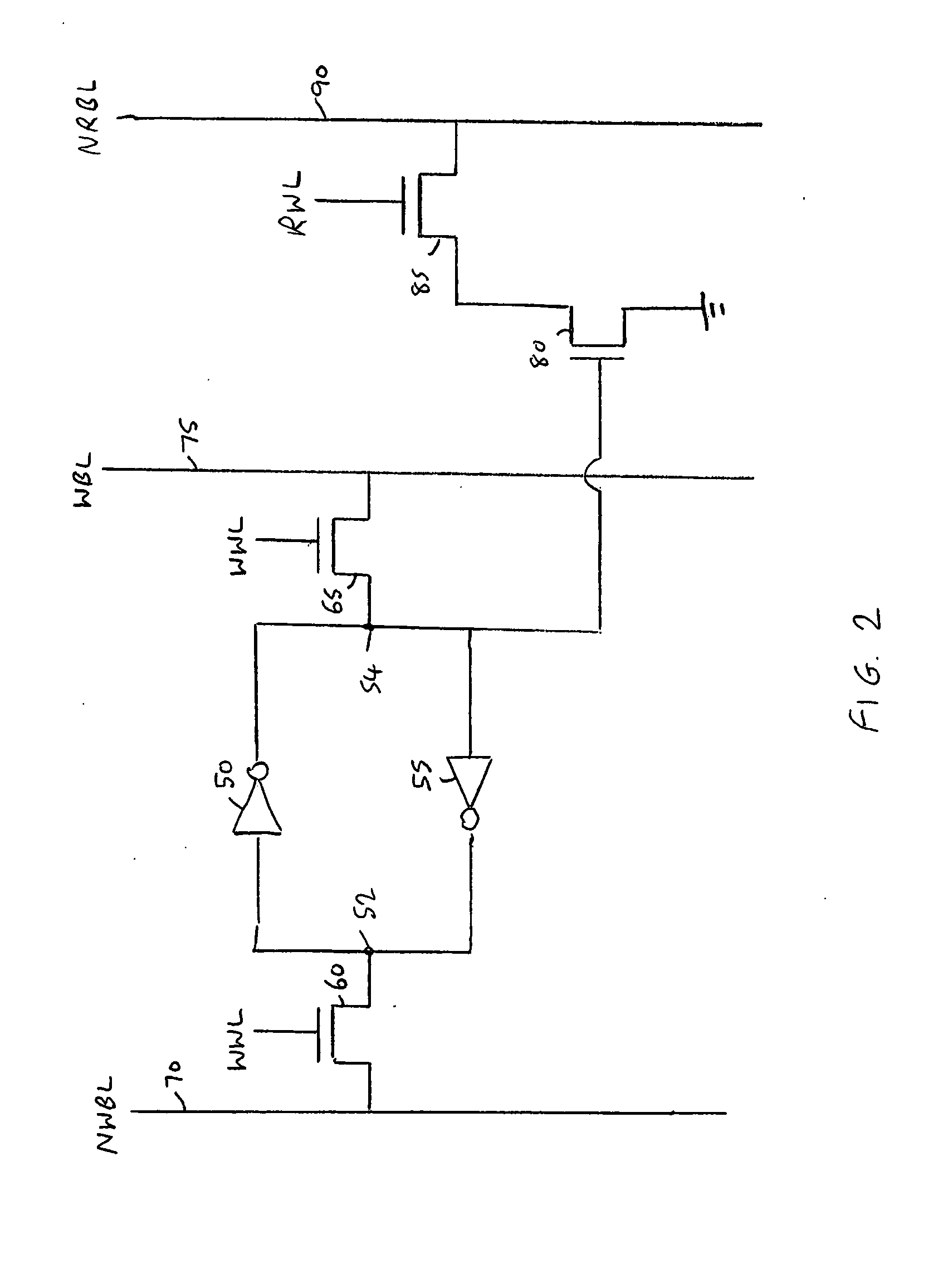
[0031]As mentioned earlier, as process geometries shrink, the variation between the various memory cells of a memory device increases. In accordance with prior art schemes, this has typically led to a requirement to increase the pulse width of the write word line signal when performing the write operation. Furthermore, even at a particular process geometry, as the supply voltage is reduced, the variation in the cells has a more prominent effect, and in particular leads to a much wider distribution in the required pulse width of the write word line signal required to ensure correct operation of the memory cells during a write operation. This is illustrated schematically in FIG. 1, which shows how the profile of the required write word line pulse width varies dependent on whether a higher supply voltage is used (curve 10) or a lower supply voltage is used (curve 20). Typically it is required to set the pulse width of the write word line select signal having regards to a worst case, an...


PUM


Abstract

A memory device and method are provided incorporating a technique for controlling a write operation within the memory device. The memory device has an array of memory cells, each memory cell supporting writing and simultaneous reading of that memory cell. Write circuitry is arranged, during a write operation, to provide write data to a number of addressed memory cells within the array, whilst word line select circuitry is responsive to the start of the write operation to assert a write word line signal that enables those addressed memory cells to store the write data. Comparing circuitry is arranged, during the write operation, to compare the write data with data currently stored in the addressed memory cells. On detecting that the write data matches the data currently stored in the addressed memory cells, the comparing circuitry asserts a control signal to the word line select circuitry to cause the word line select circuitry to de-assert the write word line signal. As a result, the pulse width of the asserted write word line signal is dependent on time taken by the addressed memory cells to store the write data, thereby leading to a significant reduction in the size of the pulse width when compared with known prior art techniques.

Description

BACKGROUND OF THE INVENTION[0001]1. Field of the Invention[0002]The present invention relates to a memory device, and method of operation of such a device, and in particular to techniques for controlling a write operation within a memory device.[0003]2. Description of the Prior Art[0004]As process geometries shrink in modern data processing systems, the variability in the operating characteristics of the individual circuit elements increases. Considering as an example a memory device consisting of an array of memory cells, it will be understood that each memory cell will typically consist of a number of electronic components such as transistors, and the variability in those individual components significantly increases as process geometries shrink. To ensure correct operation of the memory device, it is necessary to control the operation of the memory device having regards to the worst case characteristics of the memory cells within the device.[0005]Furthermore, there is an increasi...

Claims


Application Information

Patent Timeline
Patent Type & Authority Applications(United States)
IPC IPC(8): G11C7/10
CPCG11C8/08G11C11/419G11C11/418G11C11/412
Inventor CHANDRA, VIKASKIM, DAEYEON
Owner ARM LTD
Why Eureka
Try Eureka