

Light-Emitting Device and Lighting Device
a technology of light-emitting devices and lighting devices, which is applied in the direction of organic semiconductor devices, semiconductor devices, electrical apparatus, etc., can solve the problems of increasing limiting the improvement of power efficiency, and increasing the evaporation time spent for formation of light-emitting layers, so as to achieve high power efficiency and reduce the amount of organic materials used in light-emitting layers. , the effect of high power efficiency
- Summary
- Abstract
- Description
- Claims
- Application Information
AI Technical Summary
Benefits of technology
Problems solved by technology
Method used
Image

Examples
embodiment 1
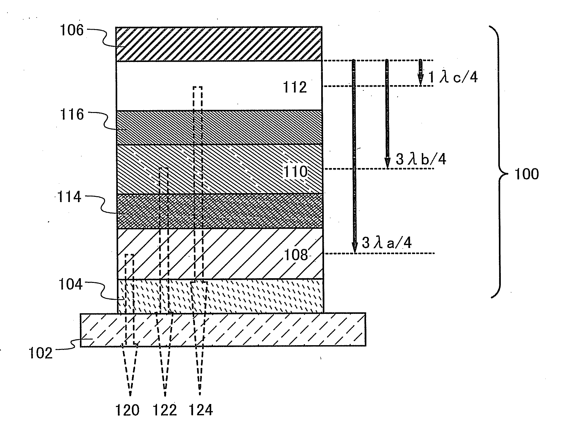
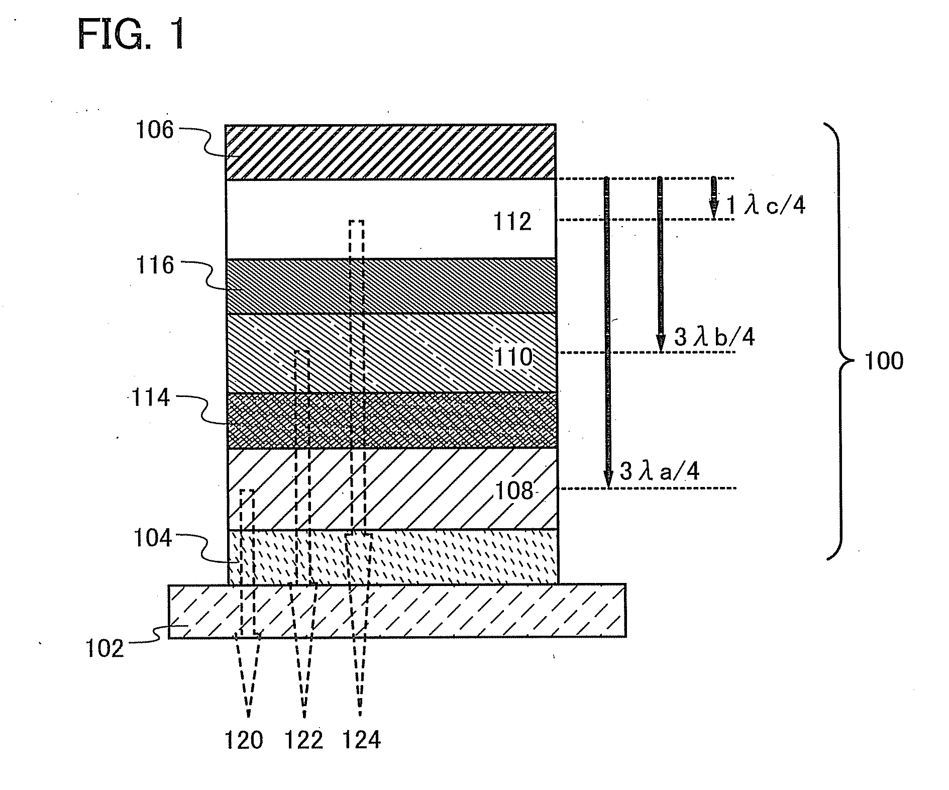
[0041]In this embodiment, an example of a structure of a light-emitting element will be described with reference to FIG. 1.
[0042]A light-emitting element 100 illustrated in FIG. 1 includes a light-transmitting electrode 104 and a light-reflecting electrode 106, and further a first light-emitting layer 108, a second light-emitting layer 110, a third light-emitting layer 112, a first intermediate layer 114, and a second intermediate layer 116 between the light-transmitting electrode 104 and the light-reflecting electrode 106. The first light-emitting layer 108 is located between the light-transmitting electrode 104 and the first intermediate layer 114. The second light-emitting layer 110 is located between the first intermediate layer 114 and the second intermediate layer 116. The third light-emitting layer 112 is located between the second intermediate layer 116 and the light-reflecting electrode 106. Note that the first light-emitting layer 108, the second light-emitting layer 110, ...
embodiment 2
[0065]In this embodiment, an example of a structure of a light-emitting element will be described with reference to FIG. 1. In this embodiment, a specific structure of the light-emitting element 100 illustrated in FIG. 1 and described in Embodiment 1 will be described.
[0066]As described in Embodiment 1, the light-emitting element 100 illustrated in FIG. 1 is provided over a substrate 102, includes the light-transmitting electrode 104 and the light-reflecting electrode 106, and includes the first light-emitting layer 108, the second light-emitting layer 110, the third light-emitting layer 112, the first intermediate layer 114, and the second intermediate layer 116 between the light-transmitting electrode 104 and the light-reflecting electrode 106. The first light-emitting layer 108 is provided between the light-transmitting electrode 104 and the first intermediate layer 114. The second light-emitting layer 110 is provided between the first intermediate layer 114 and the second interm...
embodiment 3
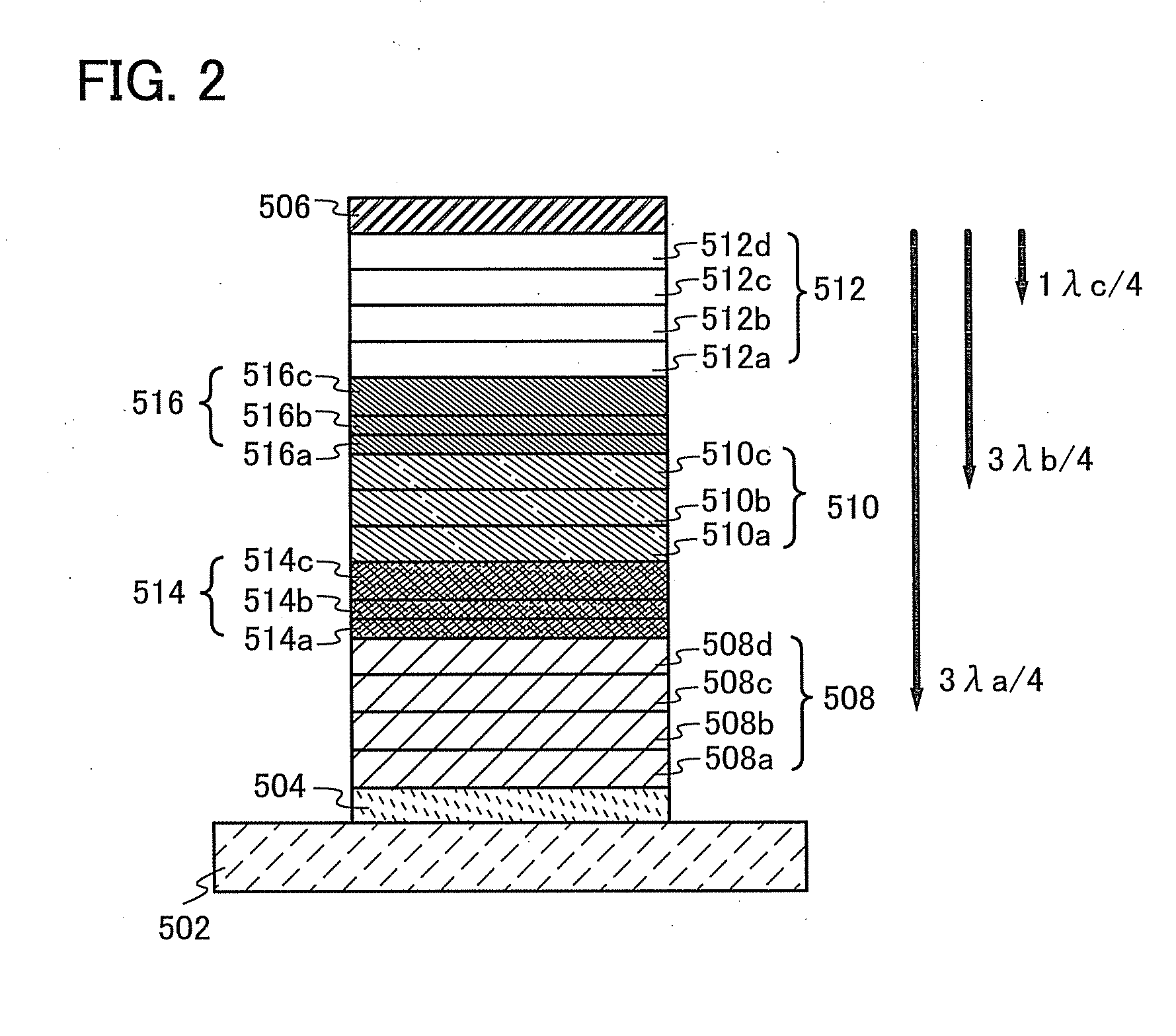
[0097]In this embodiment, a light-emitting element having a different structure from that of the light-emitting element in Embodiment 1 and Embodiment 2 will now be described with reference to FIG. 2.
[0098]The light-emitting element illustrated in FIG. 2 is provided over a substrate 502; includes a light-transmitting electrode 504 and a light-reflecting electrode 506; and includes, between the light-transmitting electrode 504 and the light-reflecting electrode 506, a first light-emitting layer 508 including a hole-injection layer 508a, a hole-transport layer 508b, a light-emitting layer 508c, and an electron-transport layer 508d; a first intermediate layer 514 including an electron-injection buffer layer 514a, an electron-relay layer 514b, and a charge-generation layer 514c; a second light-emitting layer 510 including a hole-transport layer 510a, a light-emitting layer 510b, and an electron-transport layer 510c; a second intermediate layer 516 including an electron-injection buffer ...
PUM
 Abstract
Description
Claims
Application Information