Access transistor with a buried gate

Active Publication Date: 2012-09-27
AVALANCHE TECH
View PDF2 Cites 32 Cited by
  • Summary
  • Abstract
  • Description
  • Claims
  • Application Information

AI Technical Summary

Benefits of technology

[0016]FIG. 6 shows a high level diagram of the array 10

Problems solved by technology

Such a configuration limits efficient use of the surface of the silicon substrate and results in a large memory cell size.
Problems with the memory cell includes low drive current, the current required to effectively access the MTJ, punch through leakage due to the short channel and lack of sufficient space for making contact in between.

Method used


Image

  • Access transistor with a buried gate
  • Access transistor with a buried gate
  • Access transistor with a buried gate

Examples


Embodiment Construction

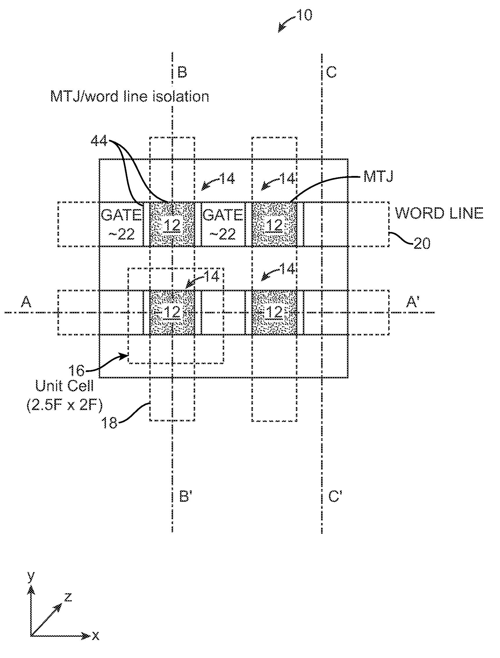
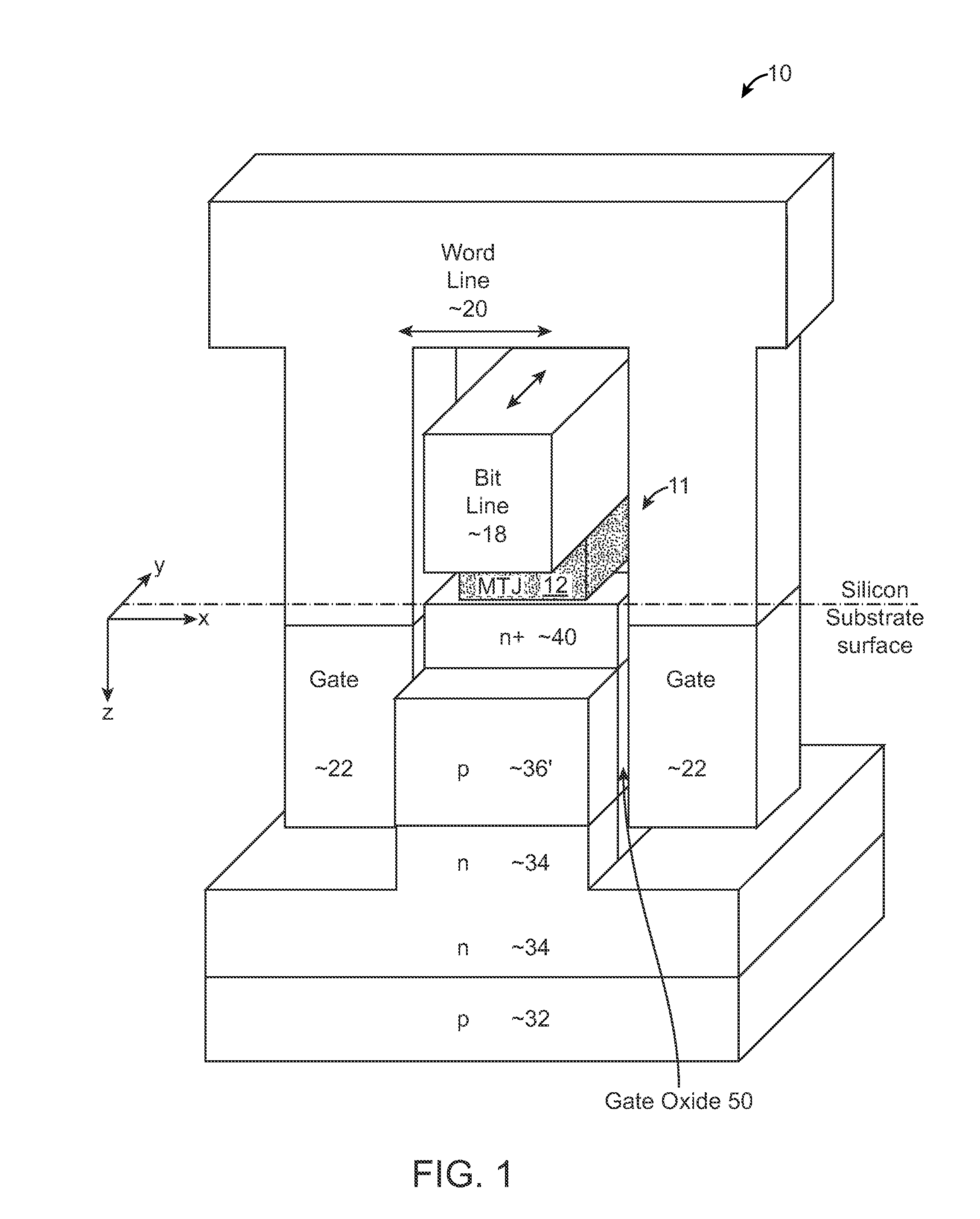
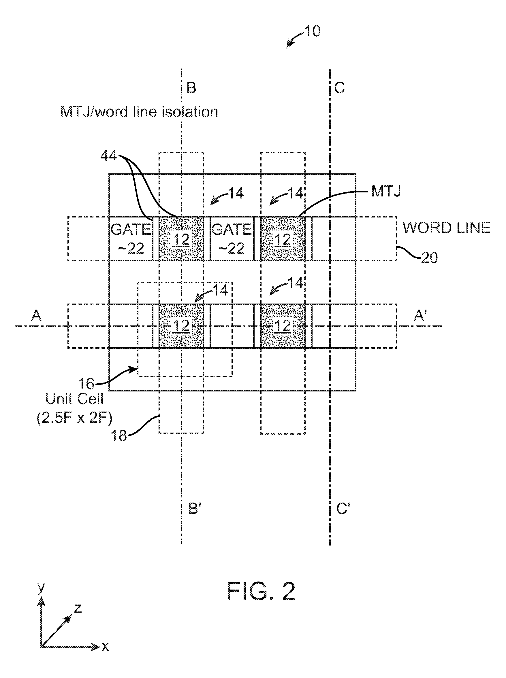
[0018]In the following description of the embodiments, reference is made to the accompanying drawings that form a part hereof, and in which is shown by way of illustration of the specific embodiments in which the invention may be practiced. It is to be understood that other embodiments may be utilized because structural changes may be made without departing from the scope of the present invention. It should be noted that the figures discussed herein are not drawn to scale and thicknesses of lines are not indicative of actual sizes.

[0019]In an embodiment of the present invention, a magnetic memory cell and a method of fabricating the same are disclosed. A magnetic memory cell is formed including a magneto tunnel junction (MTJ) and an access transistor, which is used to access the MTJ in operation. The access transistor, which is formed on a silicon substrate, includes a gate, drain, and source with the gate position substantially perpendicular to the plane of the silicon substrate th...


PUM


Abstract

A magnetic memory cell is formed including a magneto tunnel junction (MTJ) and an access transistor, which is used to access the MTJ in operation. The access transistor, which is formed on a silicon substrate, includes a gate, drain and source with the gate position substantially perpendicular to the plane of the silicon substrate thereby burying the gate and allowing more surface area on the silicon substrate for formation of additional memory cells.

Description

BACKGROUND OF THE INVENTION[0001]1. Field of the Invention[0002]The present invention relates generally to an access transistor used to access memory and method of fabricating the same, and more particularly to an access transistor with a small form factor.[0003]2. Description of the Prior Art[0004]Magnetic random access memory (MRAM) is rapidly gaining popularity as its use in replacing conventional memory is showing promise. Magnetic tunnel junctions (MTJs), which are essentially the part of the MRAM that store information, include various layers that determine the magnetic behavior of the device. An MTJ is typically formed with an accompanying access transistor used to select (or access) the MTJ for programming and / or reading. The MTJ and access transistor are herein referred to as a “magnetic memory cell”. Currently, the size of such a combination is typically 14F2, with “F” representing feature size. Such a form factor prevents magnetic memory cells from readily replacing other...

Claims


Application Information

Patent Timeline
IPC IPC(8): H01L29/82
CPCH01L27/228H01L43/02H01L29/7827H01L29/66666H10B61/22H10N50/80
Inventor SATOH, KIMIHIROABEDIFARD, EBRAHIM
Owner AVALANCHE TECH
Why Eureka
Try Eureka