Antenna device, circuit board and memory card
- Summary
- Abstract
- Description
- Claims
- Application Information
AI Technical Summary
Benefits of technology
Problems solved by technology
Method used
Image

Examples
first embodiment
(Antenna Device and Circuit Board)
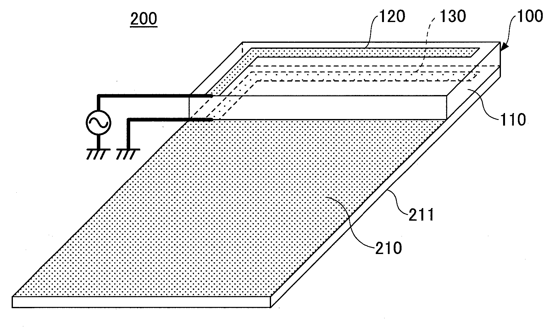
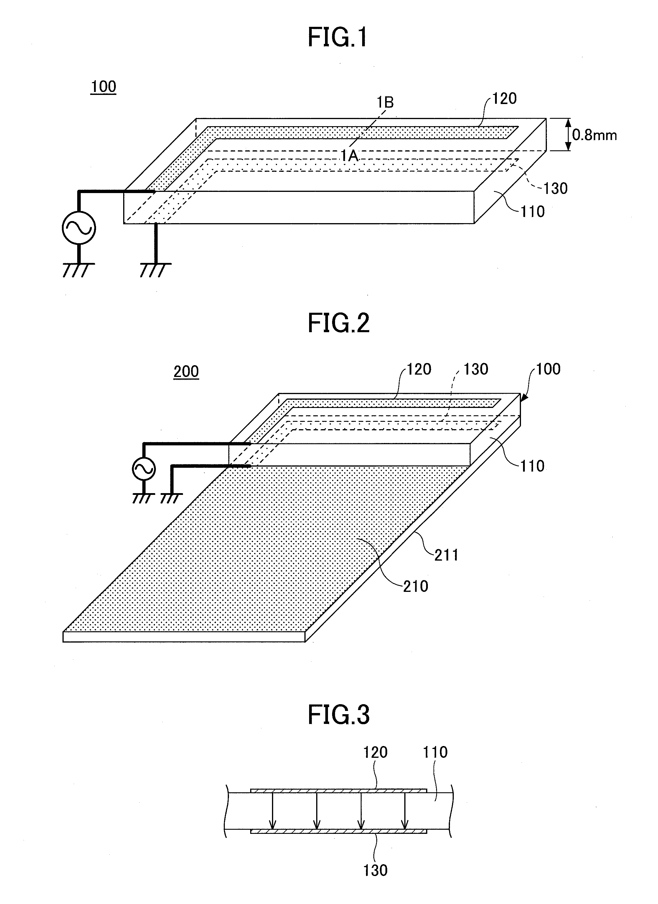
[0094]The antenna device and the circuit board of the First Embodiment are described. Referring to FIG. 1, the antenna device 100 of the First Embodiment has an antenna element 120 on one side of a substrate such as a printed-wiring board 110, and a ground element 130 on the other side of the substrate. The sides are determined relative to a thickness center of the substrate such as the printed-wiring board 110.
[0095]The antenna element 120 and the ground element 130 are made of a metallic material such as copper. The antenna element 120 and the ground element 130 are symmetrical with respect to the printed-wiring board 110. The ground element 130 of the antenna device 100 is grounded, and a high-frequency voltage of, for example, 2.4 GHz to 2.5 GHz is applied to the antenna element 12.
[0096]The antenna device of the First Embodiment may be used for communications in a frequency range of 2.4 GHz to 2.5 GHz, in wireless LAN or in Bluetooth (BT) (“Blu...
second embodiment
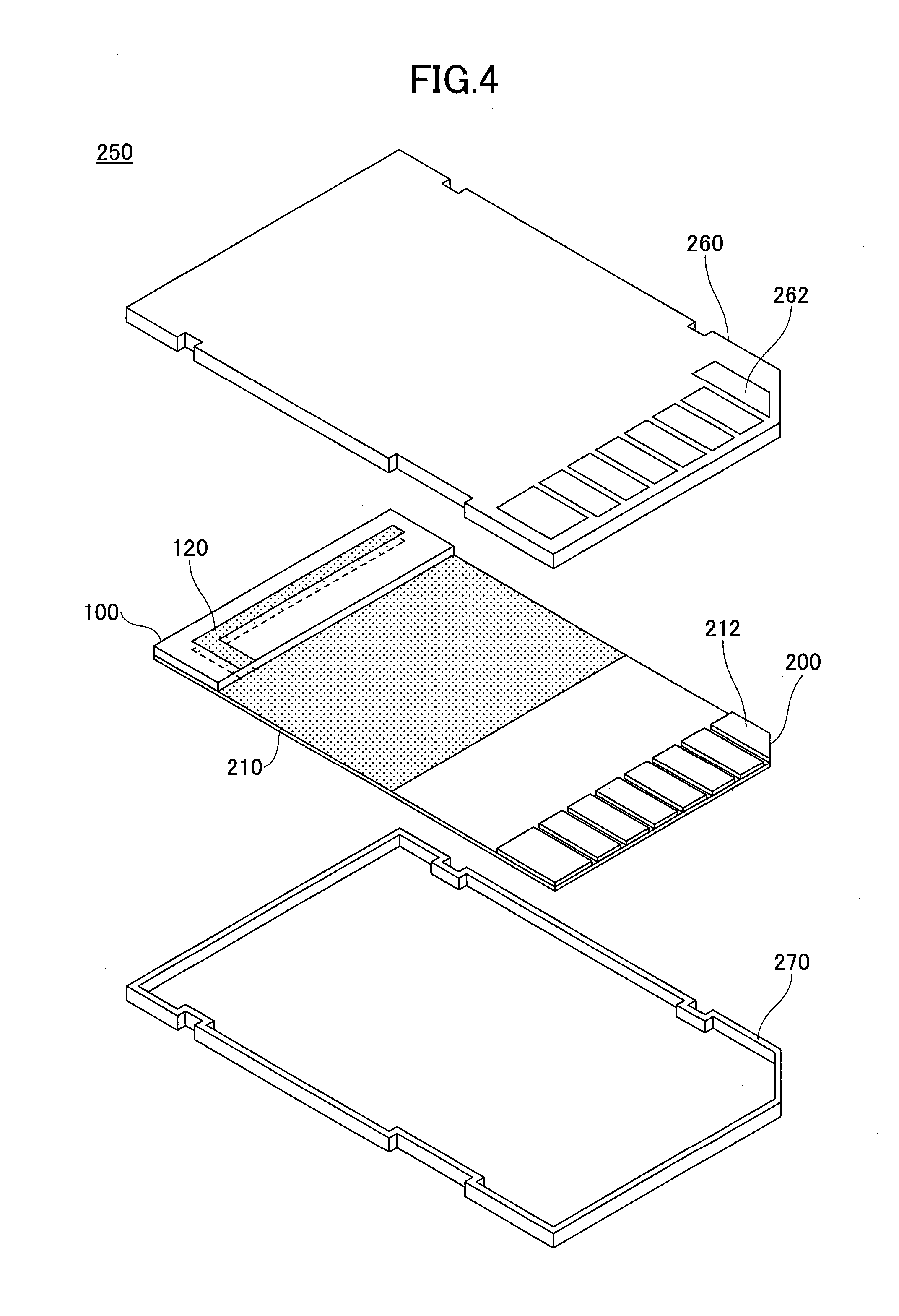
[0121]The Second Embodiment is described next. In the Second Embodiment, the circuit board and the memory card in which the antenna device is installed are described. Referring to FIG. 19, an antenna device 103 of a circuit board 202 of the Second Embodiment includes an antenna element 122 formed on one surface of a printed-wiring board 110 and a ground element 132 formed in the other surface of the printed-wiring board 110 in its entirety. The antenna element 122 includes a first side antenna element 123 on a side surface of the printed-wiring board 110 and a second side surface antenna element 124 on the side surface of the printed-wiring board 110 to thereby form an inverse F shape (hereinafter, the antenna formed in the inverse F shape may be referred to as the antenna of the inverse F type). The first side antenna element 123 is connected to the ground element 132 formed on the printed-wiring board 110 so as to be applied with a high-frequency voltage greater than that to the a...
third embodiment
[0125]The Third Embodiment is described next. An antenna device 104 of the Third Embodiment is a dipole antenna in which an antenna element and a ground element are connected. Specifically, referring to FIG. 23, a connecting portion 140 made of a metal such as copper is formed inside a through hole provided in a printed-wiring board 110 to connect the antenna element 20 to the ground element 130. Thus, the dipole element is formed. As described, by connecting the antenna element 120 to the ground element 130 by the connecting portion 140, the equivalent circuit becomes as illustrated in FIG. 24 enabling adjusting resonance.
[0126]A position where the connecting portion 140 (the throughhole) is determined by a resonance frequency or the like. For example, referring to FIG. 25, the throughhole may be formed on end portions of the antenna element 120 and the ground element 130 and the connecting portion 140 is formed in the throughhole to thereby connect the antenna element 120 to the g...
PUM
 Abstract
Description
Claims
Application Information
 - R&D Engineer
- R&D Manager
- IP Professional
- Industry Leading Data Capabilities
- Powerful AI technology
- Patent DNA Extraction
Browse by: Latest US Patents, China's latest patents, Technical Efficacy Thesaurus, Application Domain, Technology Topic.
© 2024 PatSnap. All rights reserved.Legal|Privacy policy|Modern Slavery Act Transparency Statement|Sitemap