Optical device sealing structure and optical deveice manufacturing method

a technology of sealing structure and optical device, which is applied in the direction of instruments, cladded optical fibres, transportation and packaging, etc., can solve the problems of time and cost, and the optical device may not be sealed in such a state, so as to reduce the cost of components, reduce the cost of members, and improve the sealing

Active Publication Date: 2012-10-04
SUMITOMO OSAKA CEMENT CO LTD
View PDF4 Cites 0 Cited by
  • Summary
  • Abstract
  • Description
  • Claims
  • Application Information

AI Technical Summary

Benefits of technology

[0013]According to the optical device sealing structure of the invention, the Zn-containing surface which is formed on the surface of the bare fiber portion may be strongly bonded to the Sn-containing sealing material. Thus, since there is no need to use an expensive material such as an Au which is used usually, the cost of component may be reduced and a satisfactory sealing property may be obtained.
[0014]Further, according to the optical device manufacturing method of the invention, the through hole is sealed by charging solder thereinto after forming the Zn-containing surface on the surface of the bare fiber portion by dipping or while forming the Zn-containing surface. Accordingly, since the expensive material such as Au which is used usually does not need to be used and a plating does not need to be partly formed on the bare fiber portion using a mask pattern or the like, it is possible to manufacture an optical device that enables a decrease in the cost of members and simplicity in the process and has a satisfactory sealing property.

Problems solved by technology

In a case where the through hole through which the optical fiber is inserted is sealed by solder, since the adhesion between solder and the optical fiber is not good, the optical device may not be sealed in such a state.
As a result, time and cost are spent on such an operation.

Method used


Image

  • Optical device sealing structure and optical deveice manufacturing method
  • Optical device sealing structure and optical deveice manufacturing method
  • Optical device sealing structure and optical deveice manufacturing method

Examples


first embodiment

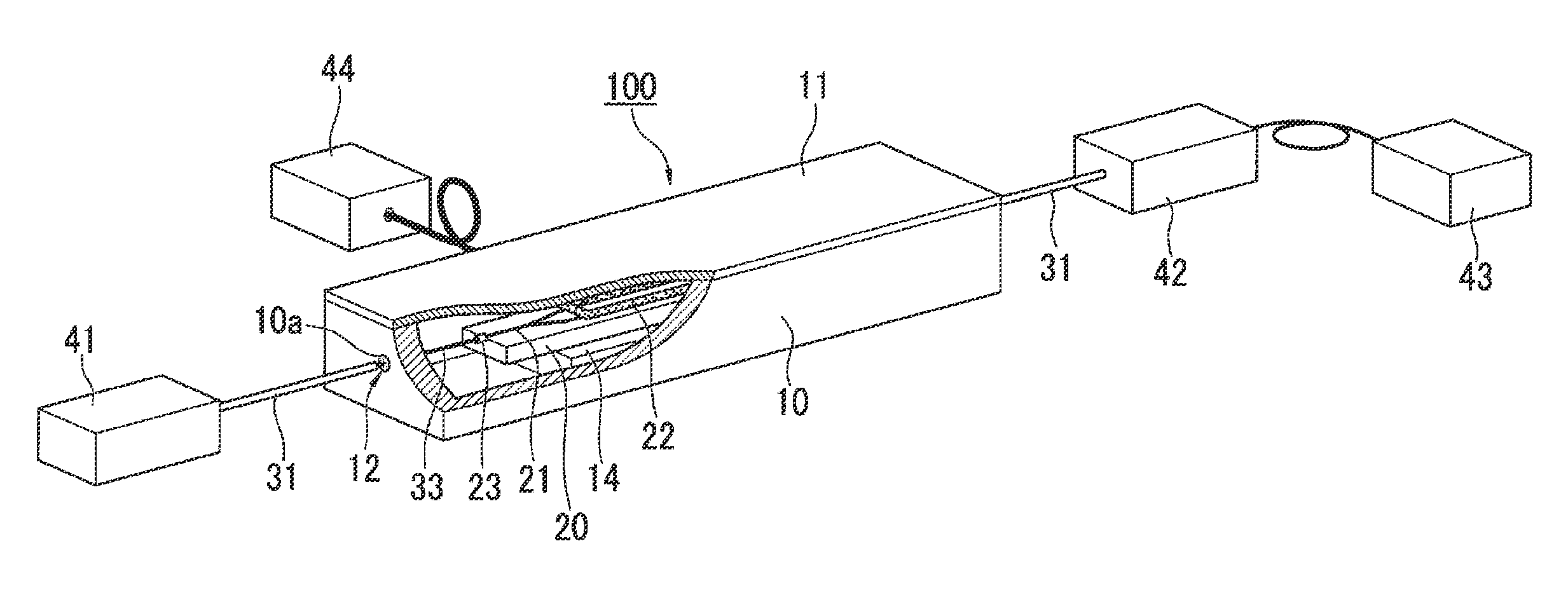
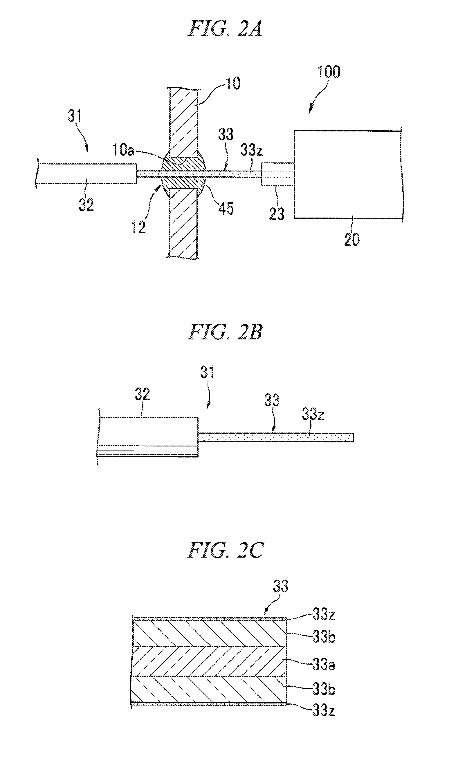
[0022]FIG. 1 is a diagram illustrating an optical waveguide package which is an embodiment of an optical device of the invention. FIGS. 2A to 2C are diagrams illustrating an optical waveguide package sealing structure.

[0023]An optical waveguide package (an optical device) 100 shown in FIG. 1 includes: a bottomed box-like case 10; an optical waveguide element (an optical element) 20 that is mounted into the case 10; a cover portion 11 that covers the opening end of the case 10 so as to be fixed thereto; and input and output optical fibers 31 that is connected to the optical waveguide element 20.

[0024]Furthermore, in FIG. 1, the case 10 and the cover portion 11 are partly notched so that the optical waveguide element 20 mounted therein is visible from the outside.

[0025]The optical waveguide element 20 is formed by installing a Mach-Zehnder optical waveguide 21 and an electrode 22 on a substrate which is formed of lithium niobate (LiNbO3; LN), and is fixed to a seat 14 inside the case ...

second embodiment

[0056]Next, a second embodiment will be described with reference to FIGS. 4A to 4C.

[0057]FIGS. 4A to 4C are diagrams illustrating an optical waveguide package manufacturing method according to the second embodiment.

[0058]The manufacturing method of the embodiment includes: forming the bare fiber portion 33 in which the bare fiber is exposed by partly removing the coating of the optical fiber 31; applying the Zn-containing solder 46 to the bare fiber portion 33; and inserting the optical fiber 31 into the through hole 10a of the case 10 and charging the Sn-containing soldering material 45 between the Zn-containing solder 46 on the bare fiber portion 33 and the inner wall of the through hole 10a.

[0059]First, as shown in FIG. 4A, the bare fiber portion 33 is formed in the optical fiber 31. The detailed procedure is the same as that of the above-described first embodiment.

[0060]Next, as shown in FIG. 4B, the Zn-containing solder 46 is partly applied to a predetermined position on the b...

third embodiment

[0070]Next, a third embodiment will be described by referring to FIGS. 5A and 5B.

[0071]FIGS. 5A and 5B are diagrams illustrating a method of manufacturing an optical waveguide package according to the third embodiment.

[0072]The manufacturing method of the embodiment includes: forming the bare fiber portion 33 in which the bare fiber is exposed by partly removing the coating of the optical fiber 31; and inserting the optical fiber 31 into the through hole 10a of the case 10 and charging the Zn-containing solder 46 between the bare fiber portion 33 and the inner wall of the through hole 10a.

[0073]First, as shown in FIG. 5A, the bare fiber portion 33 is formed in the optical fiber 31. The detailed procedure is the same as that of the above-described first embodiment.

[0074]Next, as shown in FIG. 5B, the bare fiber portion 33 of the optical fiber 31 is inserted into the through hole 10a of the case 10, and then the end portion of the bare fiber portion 33 is inserted into the connection...


PUM

PropertyMeasurementUnit
adhesionaaaaaaaaaa
adhesion strengthaaaaaaaaaa
timeaaaaaaaaaa

Abstract

To provide an optical device sealing structure capable of simply sealing an optical fiber inserting portion. Provided is a structure that seals an optical device including a metallic case having an optical element disposed therein and an optical fiber inserted through a through hole of the case, wherein a Zn-containing surface is formed on a surface of a bare fiber portion that is formed by partly removing a coating of the optical fiber so as to expose a bare fiber, and wherein an Sn-containing sealing material is charged between the Zn-containing surface and an inner wall of the through hole.

Description

[0001]This application claims the benefit of priority to Japanese Patent Application No. 2011-079164, filed 31 Mar. 2011, which is incorporated herein by reference in its entirety.FIELD OF THE INVENTION[0002]The present invention relates to an optical device sealing structure and an optical device manufacturing method.BACKGROUND[0003]There is a known optical device in which a through hole is formed in a case accommodating an optical element and an optical fiber inserted through the through hole is connected to the optical element. In the optical device, the through hole through which the optical fiber is inserted is sealed by solder (for example, see Japanese Patent Nos. 2943760 and 2800760).SUMMARY OF THE INVENTION[0004]In a case where the through hole through which the optical fiber is inserted is sealed by solder, since the adhesion between solder and the optical fiber is not good, the optical device may not be sealed in such a state. For this reason, for the purpose of improving...

Claims


Application Information

Patent Timeline
Patent Type & Authority Applications(United States)
IPC IPC(8): B32B3/10G02B6/02
CPCG02B6/3644Y10T428/24273G02B6/4248G02B6/245
Inventor KONDOU, KATSUTOSHISHIROISHI, MASARUOOTO, KAZUHIRO
Owner SUMITOMO OSAKA CEMENT CO LTD
Why Eureka
Try Eureka