Flash-Memory Device with RAID-type Controller

a flash memory and controller technology, applied in the direction of memory adressing/allocation/relocation, instruments, error detection/correction, etc., can solve the problems of reducing the available storage capacity, channel capacity divergence, flash wearout,

Inactive Publication Date: 2012-11-01
SUPER TALENT TECH CORP
View PDF3 Cites 83 Cited by
  • Summary
  • Abstract
  • Description
  • Claims
  • Application Information

AI Technical Summary

Problems solved by technology

One limitation of NAND flash is that when storing data (writing to flash), the flash can only write from ones (1) to zeros (0).
Another limitation is that NAND flash memory has a finite number of erase cycles between 10,000 and 100,000, after which the flash wears out and becomes unreliable.
As the flash memory system wears, more b

Method used


Image

  • Flash-Memory Device with RAID-type Controller
  • Flash-Memory Device with RAID-type Controller
  • Flash-Memory Device with RAID-type Controller

Examples


Embodiment Construction

[0041]The present invention relates to an improvement in smart flash drives. The following description is presented to enable one of ordinary skill in the art to make and use the invention as provided in the context of a particular application and its requirements. Various modifications to the preferred embodiment will be apparent to those with skill in the art, and the general principles defined herein may be applied to other embodiments. Therefore, the present invention is not intended to be limited to the particular embodiments shown and described, but is to be accorded the widest scope consistent with the principles and novel features herein disclosed.

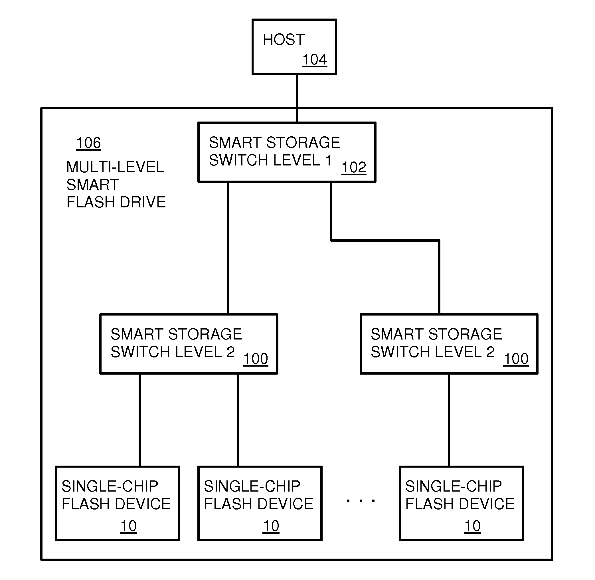
[0042]FIG. 1 shows two levels of smart storage switches using single-chip flash devices with multiple levels of integrated controllers. First-level smart storage switch 102 is part of multi-level smart flash drive 106 and connects to host 104 over a host storage bus. First-level smart storage switch 102 is connected to multiple sec...


PUM


Abstract

A smart flash drive has one or more levels of smart storage switches and a lower level of single-chip flash devices (SCFD's). A SCFD contains flash memory and controllers that perform low-level bad-block mapping and wear-leveling and logical-to-physical block mapping. The SCFD report their capacity, arrangement, and maximum wear-level count (WLC) and bad block number (BBN) to the upstream smart storage switch, which stores this information in a structure register. The smart storage switch selects the SCFD with the maximum BBN as the target and the SCFD with the lowest maximum WLC as the source of a swap for wear leveling when a WLC exceeds a threshold that rises over time. A top-level smart storage switch receives consolidated capacity, arrangement, WLC, and BBN information from lower-level smart storage switch. Data is striped and optionally scrambled by Redundant Array of Individual Disks (RAID) controllers in all levels of smart storage switches.

Description

RELATED APPLICATION[0001]This application is a divisional of the co-pending application for “Flash-Memory Device with RAID-Type Controller”, U.S. Ser. No. 13 / 197,721, filed on Aug. 3, 2011, now U.S. Pat. No. ______.[0002]This application is a continuation of the application for “Single-Chip Multi-Media Card / Secure Digital (MMC / SD) Controller Reading Power-On Boot Code from Integrated Flash Memory for User Storage”, U.S. Ser. No. 12 / 950,533, filed on Nov. 19, 2010, and U.S. Ser. No. 12 / 128,916, filed on May 29, 2008, now U.S. Pat. No. 7,552,251.[0003]This application is a continuation-in-part of “Command Queuing Smart Storage Transfer Manager for Striping Data to Raw-NAND Flash Modules”, U.S. Ser. No. 12 / 252,155, filed Oct. 15, 2008.[0004]This application is a continuation-in-part of “Hybrid 2-Level Mapping Tables For Hybrid Block- and Page-Mode Flash-Memory System”, U.S. Ser. No. 12 / 418,550, filed Apr. 3, 2009.[0005]This application is a continuation-in-part of “Multi-Level Striping...

Claims


Application Information

Patent Timeline
IPC IPC(8): G06F12/02
CPCG06F3/0604G06F3/0658G06F3/0688G06F11/1064G06F13/28G06F2212/7211G06F2213/3802G06F12/0246G06F12/0607G06F2212/7208G06F13/385
Inventor YU, FRANKMA, ABRAHAM C.CHEN, SHIMON
Owner SUPER TALENT TECH CORP
Why Eureka
Try Eureka