Grid design for iii-v compound semiconductor cell

a technology of compound semiconductor cells and grids, applied in the direction of sustainable manufacturing/processing, semiconductor devices, climate sustainability, etc., can solve the problem that the grid design of v semiconductor solar cells has not yet been designed for optimal coverag

Inactive Publication Date: 2012-11-15
SOLAERO TECH CORP
View PDF4 Cites 19 Cited by
  • Summary
  • Abstract
  • Description
  • Claims
  • Application Information

AI Technical Summary

Benefits of technology

[0008]It is an object of the present invention to provide an improved III-V compound semiconductor multijunction solar cell for terrestrial power applications with a gri

Problems solved by technology

Although III-V compound semiconductor solar cells have been widely used in satellite applications, in which their power-to-weight efficiencies are more important than cost-per-watt considerations i

Method used


Image

  • Grid design for iii-v compound semiconductor cell
  • Grid design for iii-v compound semiconductor cell
  • Grid design for iii-v compound semiconductor cell

Examples


Embodiment Construction

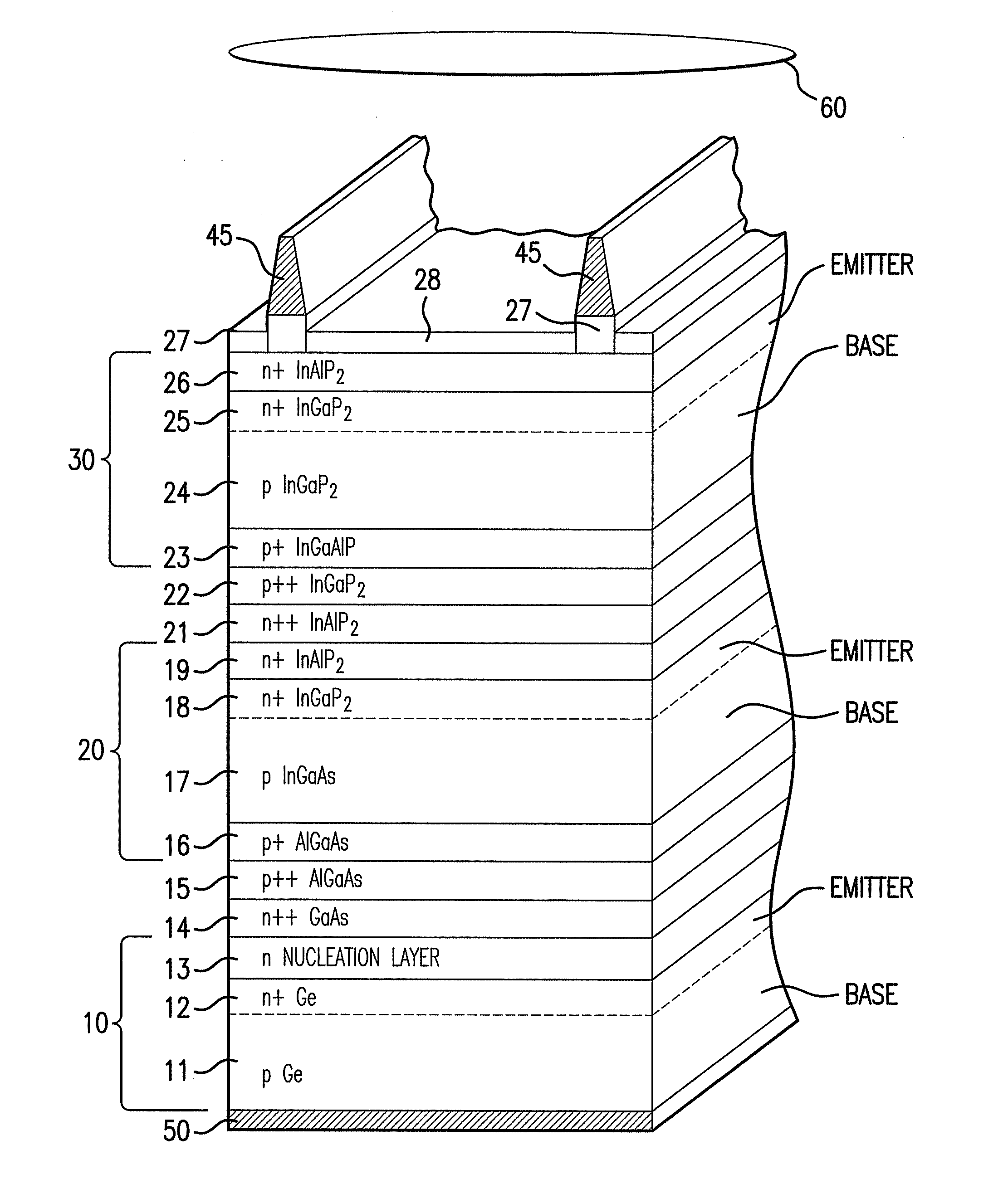
[0031]Details of the present invention will now be described including exemplary aspects and embodiments thereof. Referring to the drawings and the following description, like reference numbers are used to identify like or functionally similar elements, and are intended to illustrate major features of exemplary embodiments in a highly simplified diagrammatic manner. Moreover, the drawings are not intended to depict every feature of the actual embodiment nor the relative dimensions of the depicted elements, and are not drawn to scale.

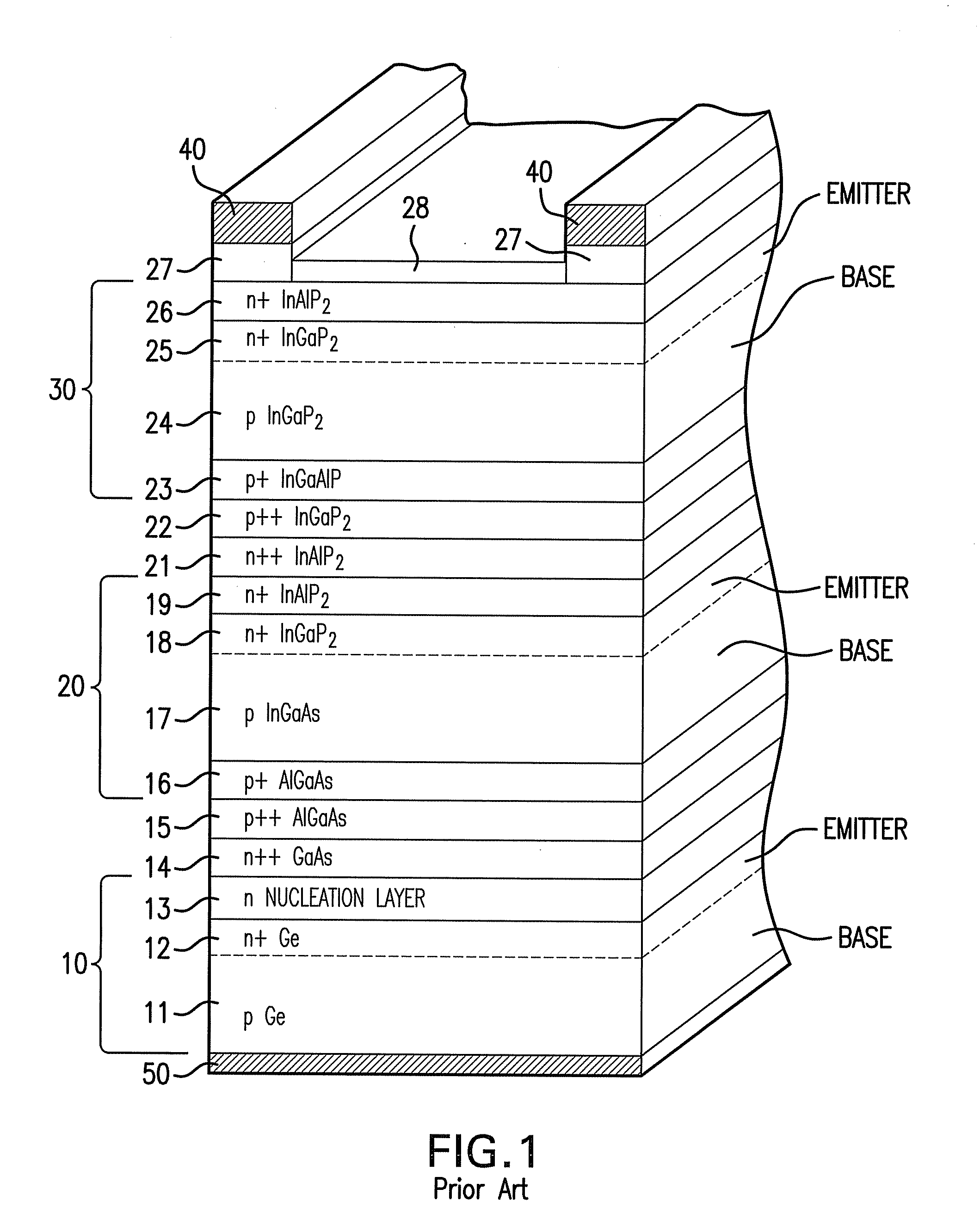
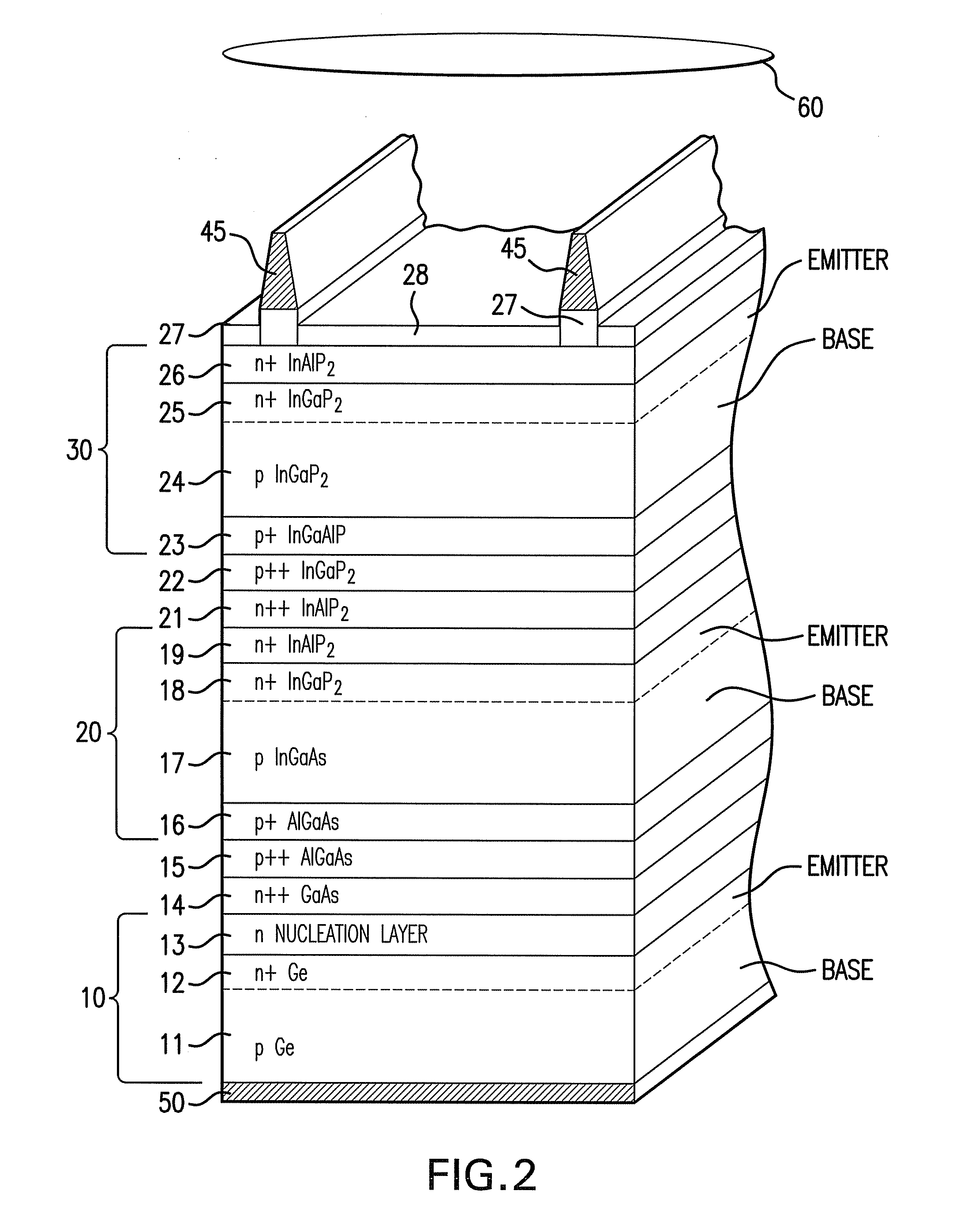
[0032]The design of a typical semiconductor structure of a triple junction III-V compound semiconductor solar cell is more particularly described in U.S. Pat. No. 6,680,432, herein incorporated by reference.

[0033]As shown in the illustrated example of FIG. 1, the bottom subcell 10 includes a substrate 11, 12 formed of p-type germanium (“Ge”), the bottom portion which also serves as a base layer of the subcell 10. A metal contact layer or pad 50 is formed...


PUM


Abstract

A photovoltaic solar cell for producing energy from the sun including a germanium substrate including a first photoactive junction and forming a bottom solar subcell; a gallium arsenide middle cell disposed on said substrate; an indium gallium phosphide top cell disposed over the middle cell; and a surface grid including a plurality of spaced apart grid lines, wherein the grid lines have a thickness greater than 7 microns, and each grid line has a cross-section in the shape of a trapezoid with a cross-sectional area between 45 and 55 square microns.

Description

BACKGROUND OF THE INVENTION[0001]1. Field of the Invention[0002]The present invention relates generally to the design of solar cells for either space or concentrator terrestrial solar power systems for the conversion of sunlight into electrical energy, and, more particularly to an arrangement including a grid configuration on the solar cell.[0003]2. Description of the Related Art[0004]Commercially available silicon solar cells for terrestrial solar power application have efficiencies ranging from 8% to 15%. Compound semiconductor solar cells, based on III-V compounds, have 28% efficiency in normal operating conditions. Moreover, it is well known that concentrating solar energy onto a III-V compound semiconductor photovoltaic cell increases the cell's efficiency to over 37% efficiency under concentration.[0005]Terrestrial solar power systems currently use silicon solar cells in view of their low cost and widespread availability. Although III-V compound semiconductor solar cells have ...

Claims


Application Information

Patent Timeline
IPC IPC(8): H01L31/06
CPCH01L31/022425H01L31/022433Y02E10/544H01L31/078Y02E10/52H01L31/0693Y02P70/50
Inventor HOFFMAN, JR., RICHARD W.PATEL, PRAVINVARGHESE, TANSEN
Owner SOLAERO TECH CORP
Why Eureka
Try Eureka