Apparatus and method for three dimensional inspection of wafer saw marks

Inactive Publication Date: 2012-11-29
KLA TENCOR CORP
View PDF4 Cites 10 Cited by
  • Summary
  • Abstract
  • Description
  • Claims
  • Application Information

AI Technical Summary

Benefits of technology

[0013]The object of the invention is to create an apparatus which provides an automatic, fast and reliable three dimensional inspection of the entire front side and / or the entire back side of a wafer with regard to saw grooves or saw marks.
[0019]It is a further object of the invention to create a method which provides an automatic, fast and reliable three dimensional inspection of the entire front side and / or the back side of wafers with regard to saw grooves or saw marks.

Problems solved by technology

One type of defect is caused by the process of sawing-off the wafer from the silicon ingot.
In many cases, the problem is that an image of a saw mark cannot be exactly extracted from a picture of the surface of a solar cell wafer as a candidate for a defect.
Therefore, it is difficult to set up a predetermined region centering on said pixel which distinguishes one image of said saw mark at a time.
The prior art methods show drawbacks.
The manual methods are slow and do not inspect all solar cell wafers.
As a result there is an insufficient detection of the defect (saw mark).
Furthermore, many prior art methods are less accurate and less repeatable.
As a consequence, the prior art methods may miss a groove completely or underestimate its depth.
This also results in an insufficient detection of the defect.
As a consequence, the inspection process is slower, more error-prone, and less flexible.

Method used


Image

  • Apparatus and method for three dimensional inspection of wafer saw marks
  • Apparatus and method for three dimensional inspection of wafer saw marks
  • Apparatus and method for three dimensional inspection of wafer saw marks

Examples


Embodiment Construction

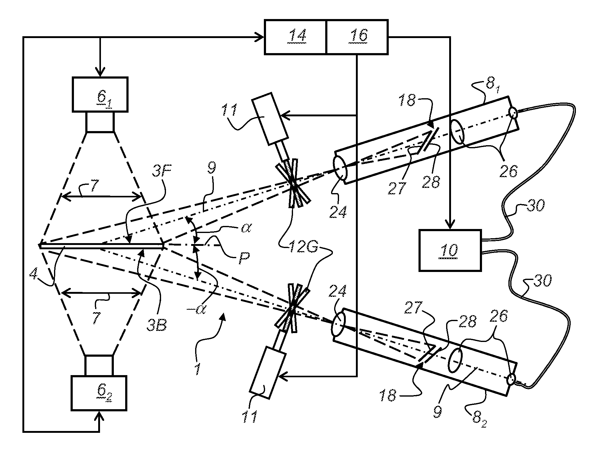
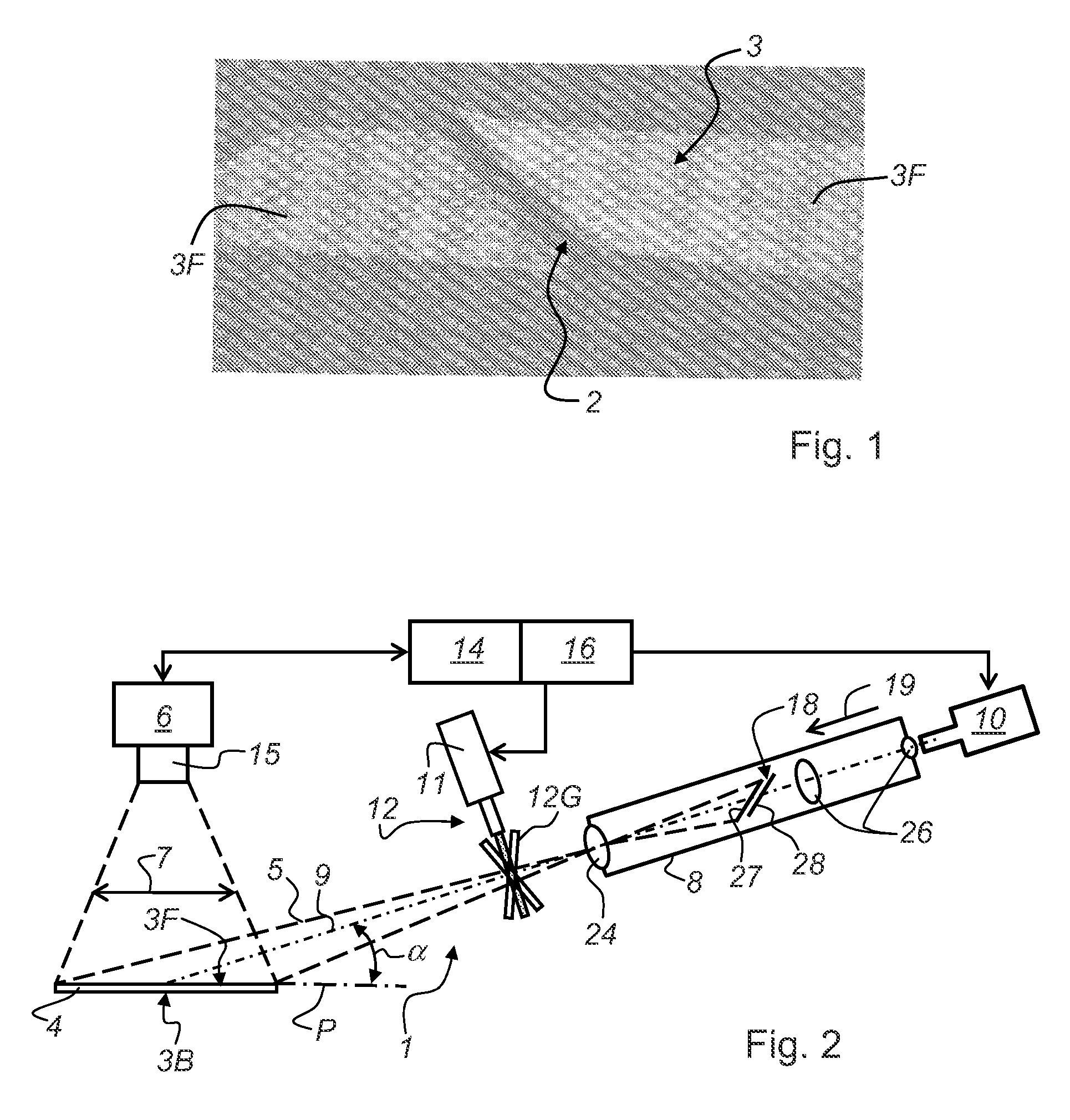
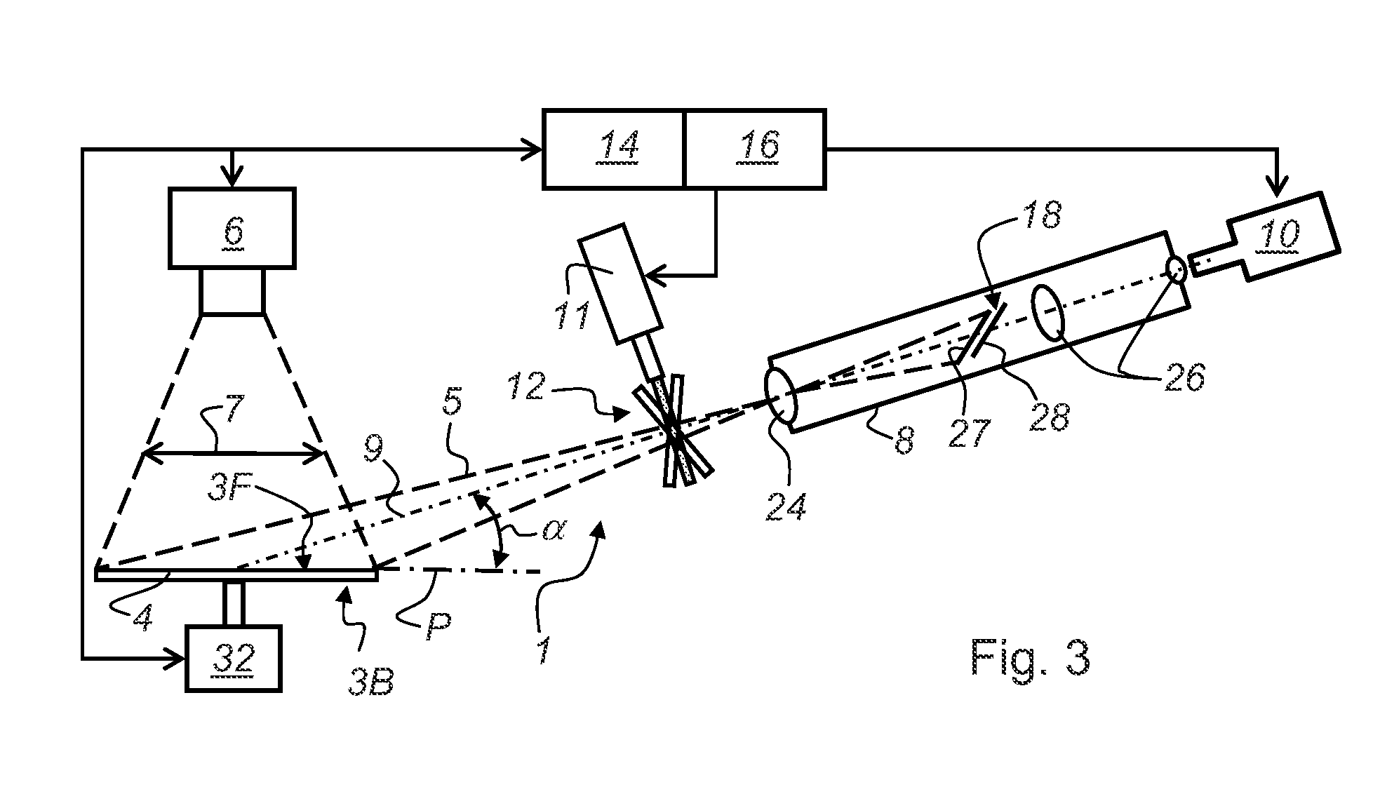
[0059]Same reference numerals refer to same elements throughout the various figures. Furthermore, only reference numerals necessary for the description of the respective figure are shown in the figures. The shown embodiments represent only examples of how the apparatus and method according to the invention can be designed. This should not be regarded as limiting the invention.

[0060]FIG. 1 shows a partial view of a saw groove on the front side 3F of a wafer 4 (see FIG. 2), wherein the saw groove 2 has a step-like shape. Silicon wafers used to manufacture photovoltaic cells need to be inspected for various defects. One type of defect is caused by the process of sawing-off the wafer from a silicon ingot (not shown). The form of the silicon ingot can be a cuboid or a cylinder. Consequently, wafer 4 is round or rectangular, respectively. Saw grooves 2 or saw marks are local, elongated and 3-dimensional departures from the normally flat front side 3F or back side 3b of wafer 4. In case wa...


PUM


Abstract

An apparatus (1) and a method for the three dimensional inspection of saw marks (2) on at least one surface (3) of a wafer (4) are disclosed. At least one camera (6) is required to capture an image of the entire surface (3) of the wafer (4). At least one line projector (8) provides a light bundle (5), centered about a central beam axis (9). The line projector (8) is arranged such that the central beam axis (9) is at an acute angle (α) with regard to the plane (P) of the wafer (4). A line shifter (12) is positioned in the light bundle (5) between each line projector (8) and the surface (3) of the wafer (4). A frame grabber (14) and an image processor (16) are used to synchronize and coordinate the image capture and the position of the pattern (20) of lines (22) on the front side (3F) and / or the back side (3B) of the wafer (4).

Description

CROSS REFERENCE TO RELATED APPLICATIONS[0001]This patent application claims priority of U.S. provisional patent application No. 61 / 368,543 filed Jul. 30, 2010, the application is incorporated herein by reference.FIELD OF THE INVENTION[0002]The present invention relates to an apparatus for the three dimensional inspection of saw marks on at least one surface of a wafer.[0003]The invention relates as well to a method for determining saw marks on at least one surface of a wafer.BACKGROUND OF THE INVENTION[0004]Silicon wafers are used to manufacture photovoltaic cells. Each silicon wafer is cut from an ingot with a specialized saw. The surface of the wafers needs to be inspected for various defects. One type of defect is caused by the process of sawing-off the wafer from the silicon ingot. Saw grooves or saw marks are local, elongated, 3-dimensional departures from the normally flat surface of the wafer. Each saw mark is extended and formed in the sliding direction of the saw and parall...

Claims


Application Information

Patent Timeline
IPC IPC(8): H04N13/02
CPCG01B11/25H01L22/12G01N21/9501G01B2210/44G01B11/30G01N21/956H01L22/00
Inventor MAISON, BENOITHILL, ANDYHERMANS, LAURENTNIJS, FRANSVAN GILS, KARELWOUTERS, CHRISTOPHE
Owner KLA TENCOR CORP
Why Eureka
Try Eureka