

Semiconductor device
a technology of semiconductor devices and metal films, applied in semiconductor devices, semiconductor/solid-state device details, electrical apparatus, etc., can solve the problems of stress at the ends of metal films, damage to the portions of surface electrodes immediately underlying these ends, and ensure sufficient reliability of semiconductor devices, so as to prevent damage to the surface electrodes
- Summary
- Abstract
- Description
- Claims
- Application Information
AI Technical Summary
Benefits of technology
Problems solved by technology
Method used
Image

Examples
first embodiment
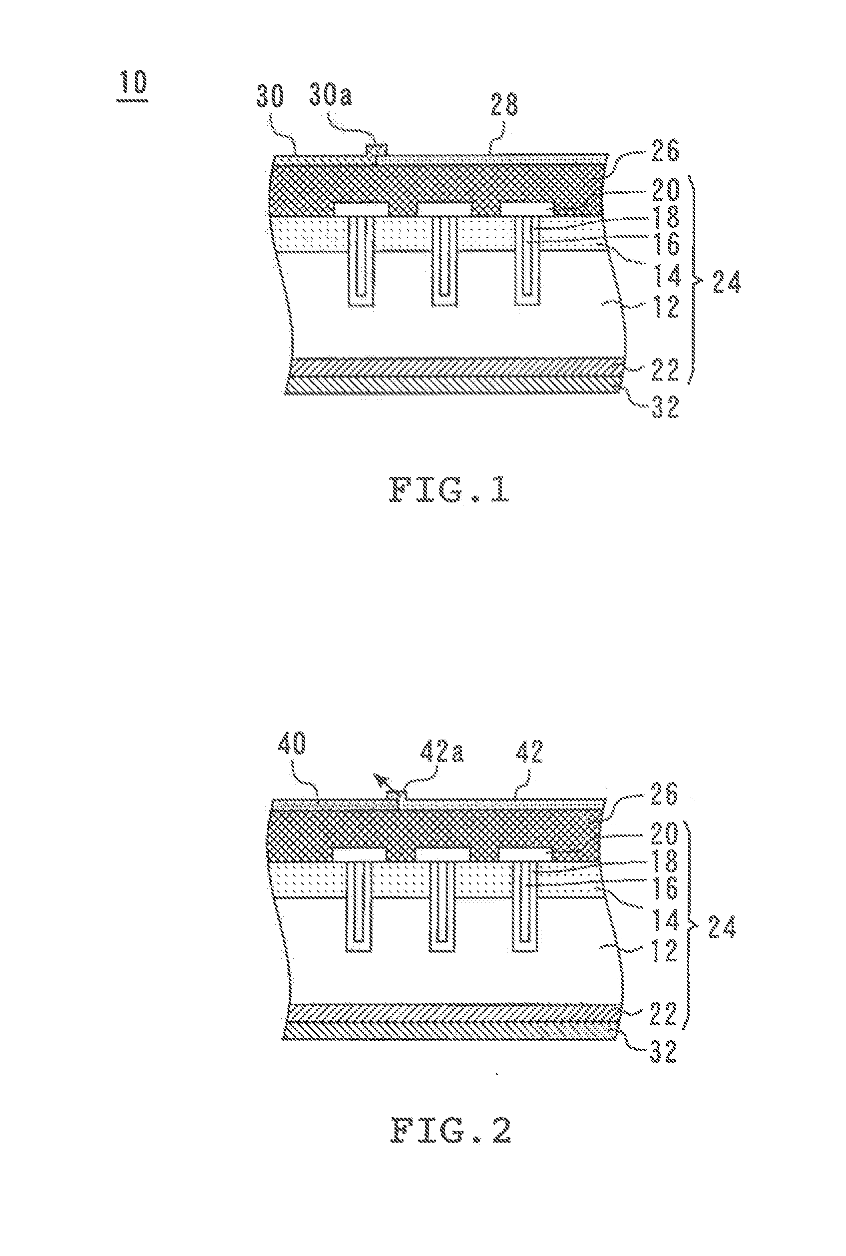
[0016]FIG. 1 is a cross-sectional view of a semiconductor device 10 in accordance with a first embodiment of the present invention. The semiconductor device 10 includes an epitaxial layer 12. Abase layer 14 is formed on the top surface of the epitaxial layer 12. Polysilicon gates 16 are formed to penetrate through the base layer 14. Each polysilicon gate 16 is covered with a gate oxide film 18 and connected to a gate 20. A collector layer 22 is formed on the bottom surface of the epitaxial layer 12. The entire structure described above is referred to herein as the substrate 24.
[0017]A surface electrode 26 of a material containing 95% or more of aluminum is formed on the substrate 24. A metal film 28 of solderable material is formed on the surface electrode 26. The metal film 28 is formed of a plurality of metals other than aluminum. An end-securing film 30 of polyimide is also formed on the surface electrode 26. The end-securing film 30 has a portion on the surface electrode 26 and ...
second embodiment
[0020]FIG. 2 is a cross-sectional view of a semiconductor device in accordance with a second embodiment of the present invention. Components of this semiconductor device which are identical to those of the semiconductor device of the first embodiment are designated by the same reference numerals and will not be further described herein.
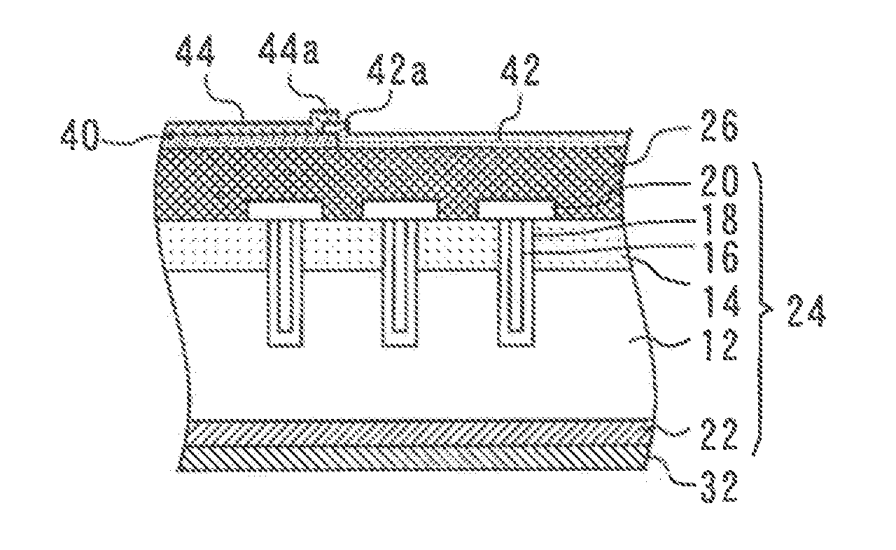
[0021]The semiconductor device of the second embodiment includes a protective film 40 formed on the surface electrode 26. The protective film 40 is a nitride film. A metal film 42 is also formed on the surface electrode 26. The metal film 42 is formed of solderable material and has a portion on the surface electrode 26 and also has a riding-up portion (or overlying portion) 42a which is formed integrally with the portion on the surface electrode 26 and which overlies (or rides up on) the ends of the protective film 40.
[0022]It should be noted that the adhesion between the metal film 42 and the protective film 40 is lower than that between the surface ...
third embodiment
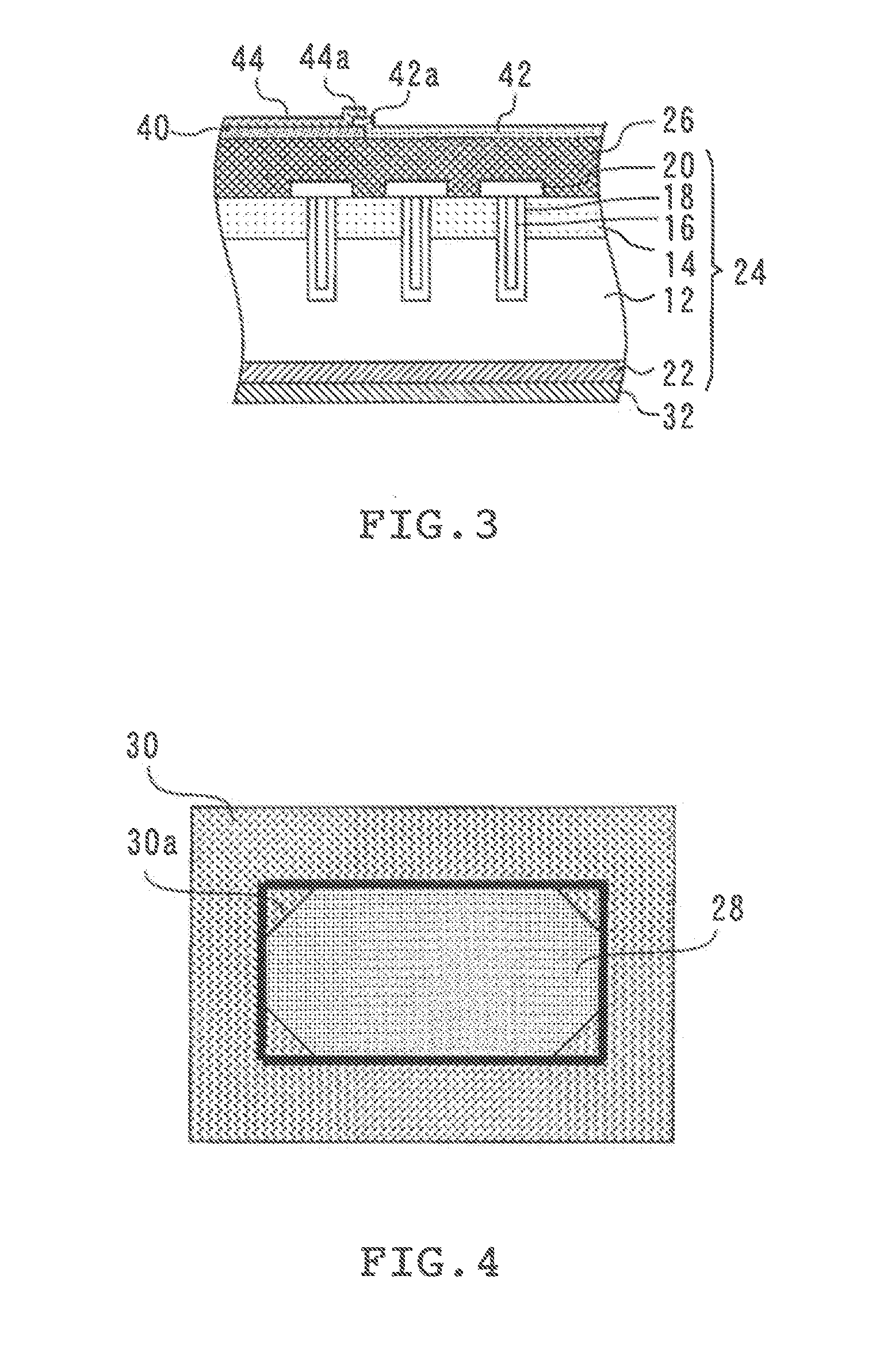
[0027]FIG. 4 is a plan view of a semiconductor device in accordance with a third embodiment of the present invention. The semiconductor device of the third embodiment is basically similar to that of the first embodiment, except that it is characterized by the configurations of the metal film and the overlapping portion of the end-securing film.
[0028]The metal film 28 is formed on the substrate 24 and has a (rectangular) configuration having corners. In FIG. 4, the thick solid line indicates the configuration of the metal film 28. The overlapping portion 30a of the end-securing film 30 is formed only on the corners of the metal film 28.
[0029]When a metal film, such as the metal film 28, has a configuration with corners, thermal stress tends to concentrate at these corners. Therefore, in the semiconductor device of the third embodiment, the overlapping portion 30a of the end-securing film 30 is formed on the corners of the metal film 28 so as to secure these corners. This prevents str...
PUM
| Property | Measurement | Unit |
|---|---|---|
| adhesion | aaaaa | aaaaa |
| thermal stress | aaaaa | aaaaa |
| stress concentration | aaaaa | aaaaa |
Abstract
Description
Claims
Application Information