Method of fabricating semiconductor memory device

a memory device and semiconductor technology, applied in the direction of semiconductor devices, electrical devices, transistors, etc., can solve the problems of affecting the uniform thickness the difficulty of achieving the narrower interval from the viewpoint of photolithography technology, and the unetched part becoming an obstacle, so as to prevent a damage at the surface of the floating gate, reduce the number of fabrication processes, and ensure the effect of quality

Inactive Publication Date: 2006-08-29
RENESAS ELECTRONICS CORP
View PDF3 Cites 0 Cited by
  • Summary
  • Abstract
  • Description
  • Claims
  • Application Information

AI Technical Summary

Benefits of technology

[0013]Accordingly, it is an object of the present invention to provide a fabrication method for a semiconductor memory device, which prevents a damage at the surface of a floating gate even if the floating gate is formed of doped polysilicon, ensures adequate programming of memory cells and reduces the number of fabrication processes.

Problems solved by technology

It is however difficult to achieve the narrower interval from the viewpoint of the resolution of the photolithography technology at the time of fabricating the floating gate.
Such a damage produces undulations at the surface of the floating gate fabricated finally, which would greatly affect the uniform thickness of the floating gate.
This results in a variation in the amount of charges stored in the floating gate, i.e., a variation in the capacitance of the floating gate in each memory cell, disabling the provision of a semiconductor memory device with an improved erasure characteristic or a reduced erasure voltage.
The unetched part therefore becomes an obstacle in increasing the capacitance of the capacitor between the control gate and the capacitance insulating layer.

Method used


Image

  • Method of fabricating semiconductor memory device
  • Method of fabricating semiconductor memory device
  • Method of fabricating semiconductor memory device

Examples


Embodiment Construction

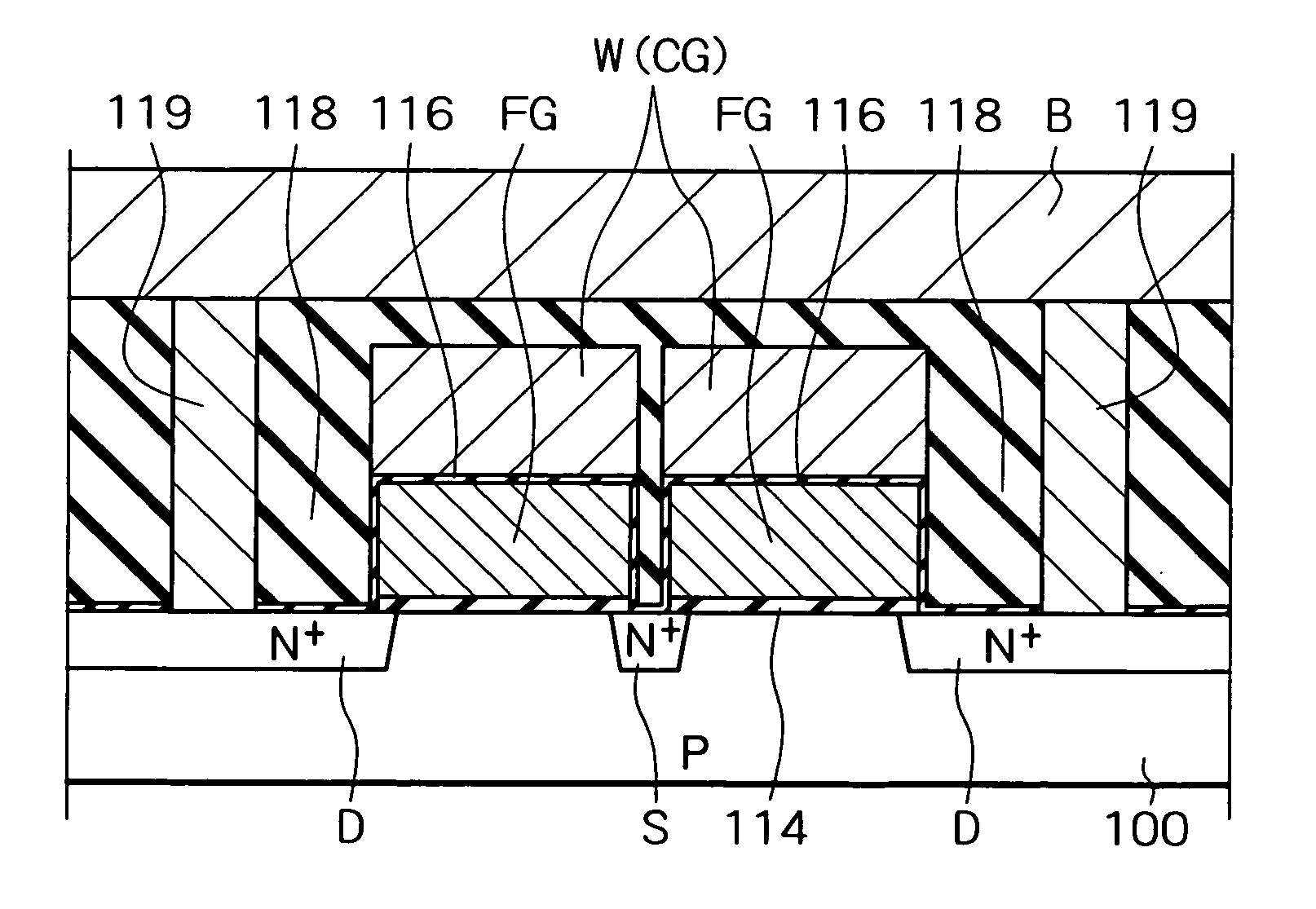
[0035]One embodiment of the present invention will be described below with reference to the accompanying drawings. FIG. 3 is a circuit diagram of a semiconductor memory device according to the invention. A flash memory FM is comprised of a plurality of stacked-gate memory cells M each having a floating gate and a control gate. The memory cells M are laid out in a matrix form in such a way that the control gates CG of those memory cells M which are laid out in the row direction are connected to respective word lines W extending in the row direction. The source regions S or drain regions D of adjoining memory cells M in those memory cells M which are laid out in the column direction are constituted as a common source region or a common drain region.

[0036]Each common source region S of the memory cells laid out in the row direction extends and is connected to GND by source contacts SC laid out at desired pitches in the row direction. Drain contacts DC are provided in each common drain ...


PUM

PropertyMeasurementUnit
thicknessaaaaaaaaaa
thicknessaaaaaaaaaa
thicknessaaaaaaaaaa

Abstract

A silicon layer doped with an impurity for a floating gate, a protective layer, a silicon nitride layer of a laminated hard mask and a first NSG layer are formed into a desired pattern, on which a second NSG layer is formed and left as a side wall. With the second NSG layer as a mask, the silicon nitride layer is etched. Using the remaining silicon nitride layer as a mask, the silicon layer is etched to form a silicon pattern whose surface is covered with a second protective layer, and the silicon nitride layer is etched out. Accordingly, it is possible to prevent a damage at the surface of the floating gate at the time of forming the floating gate using doped polysilicon.

Description

BACKGROUND OF THE INVENTION[0001]1. Field of the Invention[0002]The present invention relates to a method of fabricating a semiconductor memory device including stacked-gate nonvolatile memory cells having a floating gate and a control gate.[0003]2. Description of the Related Art[0004]A semiconductor device such as a flash memory which is recently used in a memory card or so comprises stacked-gate nonvolatile memory cells with an MOS structure wherein each memory cell has a floating gate and a control gate laminated. In this type of memory cell, data recording or erasure or so-called programming is accomplished as the threshold value of the memory cell is changed by storing charges stored in the floating gate through a tunnel oxide layer directly underlying the floating gate or removing the stored charges. It is known that to execute programming adequately, particularly, to improve the erasure characteristic or reduce the erasure voltage, the capacitor between the floating gate and ...

Claims


Application Information

Patent Timeline
Patent Type & Authority Patents(United States)
IPC IPC(8): H01L21/336H01L21/8247H01L27/115H01L29/423H01L29/788H01L29/792
CPCH01L27/115H01L29/7885H01L29/42324H01L27/11521H10B69/00H10B41/30
Inventor SUZUKI, JUNICHIKANAMORI, KOHJI
Owner RENESAS ELECTRONICS CORP
Why Eureka
Try Eureka