
Organic light-emitting display device and method of manufacturing the same

a technology of light-emitting display device and organic material, which is applied in the direction of static indicating device, electroluminescent light source, instruments, etc., can solve the problems of low power consumption, high resolution, and lightweight and thin display devi

Active Publication Date: 2012-12-13
SAMSUNG DISPLAY CO LTD
View PDF3 Cites 83 Cited by
  • Summary
  • Abstract
  • Description
  • Claims
  • Application Information

AI Technical Summary

Benefits of technology

[0008]Aspects of the present invention also provide an improved organic light-emitting display device which can be manufactured by a reduced number of deposition processes using fine metal masks.
[0009]Aspects of the present invention further provide an organic light-emitting display device which has a reduced defect rate caused by intrusion of an organic layer in a pixel into another pixel.

Problems solved by technology

Recently, there have been demands for display devices that are lightweight and thin, consume low power and provide high resolution.

Method used


Image

  • Organic light-emitting display device and method of manufacturing the same
  • Organic light-emitting display device and method of manufacturing the same
  • Organic light-emitting display device and method of manufacturing the same

Examples


Embodiment Construction

[0032]An organic light-emitting display includes a plurality of organic layers, each containing a material that emits red, green or blue light. Each of the organic layers is formed by a deposition process using a separate fine metal mask. Therefore, a number of complicated deposition processes using fine metal masks are required.

[0033]In an organic light-emitting display, if an organic layer being deposited in a target pixel using a fine metal mask intrudes into a neighboring pixel, when the neighboring pixel emits light, the organic layer may also emit light, thus causing pixel defects.

[0034]The present invention will now be described more fully hereinafter with reference to the accompanying drawings, in which preferred embodiments of the invention are shown. This invention may, however, be embodied in different forms and should not be construed as limited to the embodiments set forth herein. Rather, these embodiments are provided so that this disclosure will be thorough and comple...


PUM


Abstract

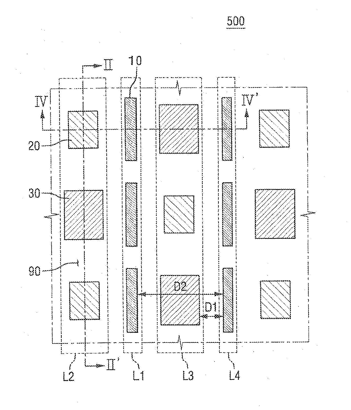
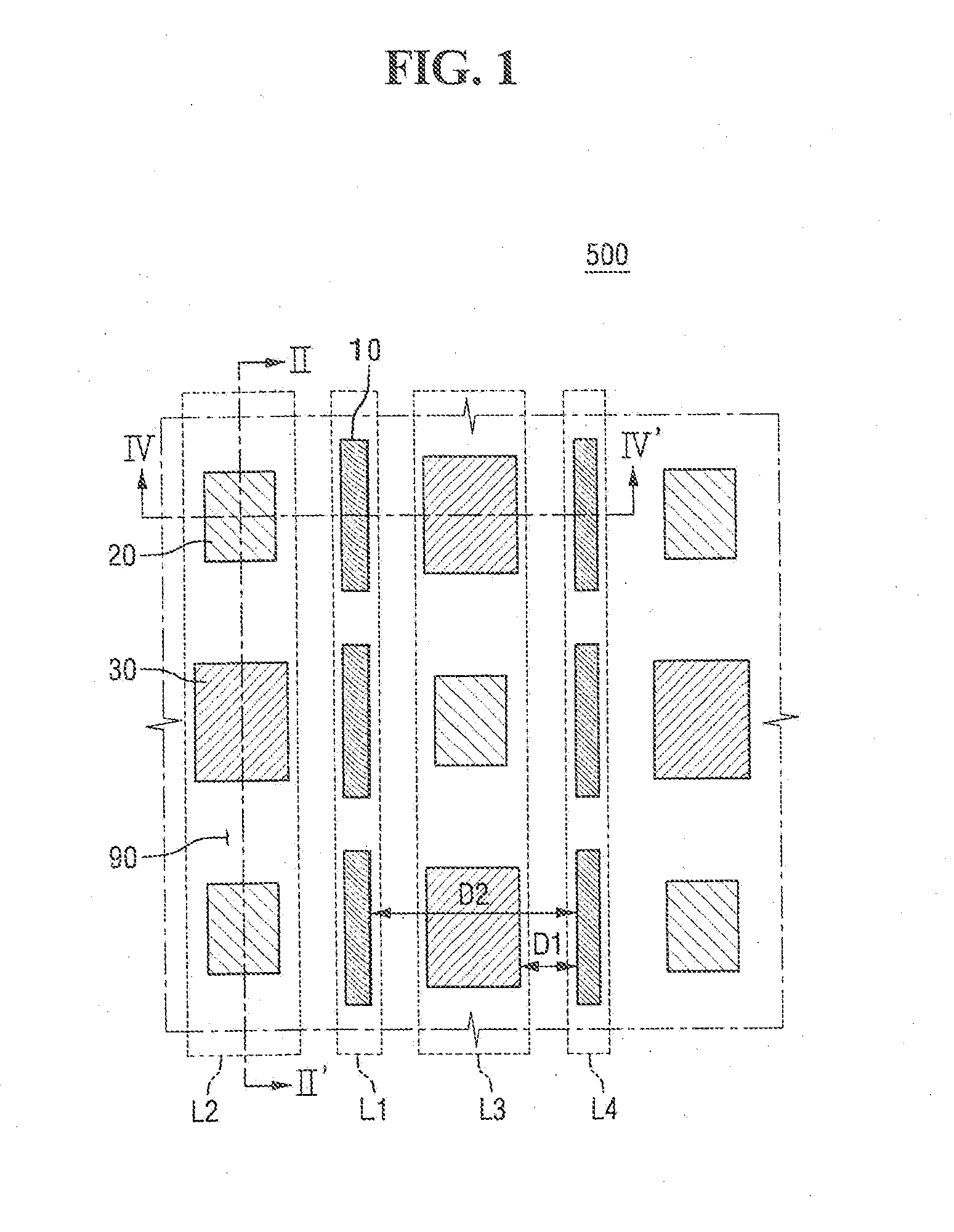
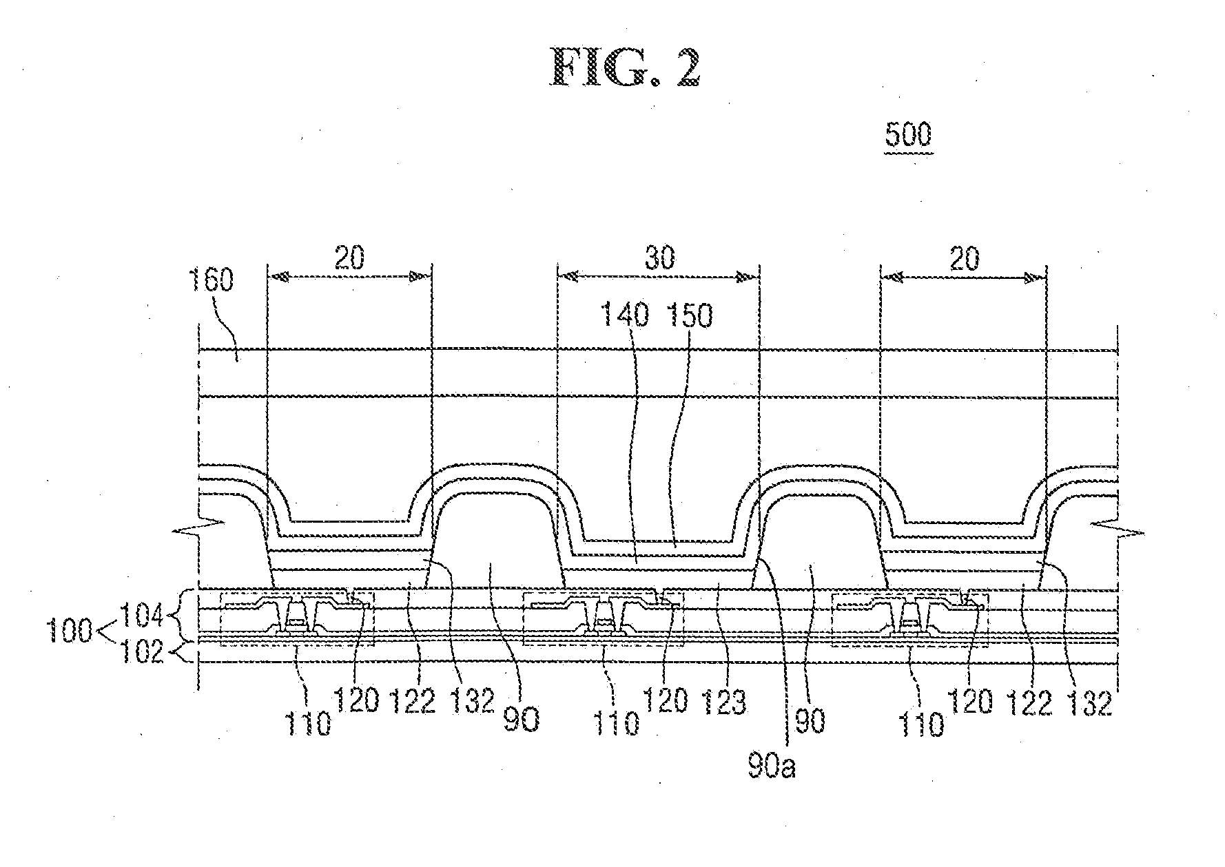
An organic light-emitting display device includes a substrate, a plurality of pixel electrodes arranged in a matrix on the substrate, and an organic common layer covering the pixel electrodes. The pixel electrodes include a plurality of first pixel electrodes, a plurality of second pixel electrodes, and a plurality of third pixel electrodes. An n-th pixel column includes the second pixel electrodes and the third pixel electrodes arranged alternately, an (n+1)-th pixel column which is adjacent to the n-th pixel column includes the first pixel electrodes, and an (n+2)-th pixel column which is adjacent to the (n+1)-th pixel column includes the second pixel electrodes and the third pixel electrodes arranged alternately, wherein n is a natural number. One of the second and third pixel electrodes is disposed in the n-th pixel column in a row and the other one of the second and third pixel electrodes is disposed in the (n+2)-th pixel column in the same row.

Description

CLAIM OF PRIORITY[0001]This application makes reference to, incorporates the same herein, and claims all benefits accruing under 35 U.S.C. §119 from an application earlier filed in the Korean Intellectual Property Office on the 13 of Jun. 2011 and there duly assigned Serial No. 10-2011-0057028.BACKGROUND OF THE INVENTION[0002]1. Field of the Invention[0003]The present invention relates to an organic light-emitting display device and a method of manufacturing the same, and more particularly, to an organic light-emitting display device including an organic common layer and a method of manufacturing the organic light-emitting display device.[0004]2. Description of the Related Art[0005]The rapid development of the information technology (IT) industry is dramatically increasing the use of display devices. Recently, there have been demands for display devices that are lightweight and thin, consume low power and provide high resolution. To meet these demands, liquid crystal displays or org...

Claims


Application Information

Patent Timeline
IPC IPC(8): G09G3/30H01L33/60
CPCH01L27/3216H01L51/525H01L27/326H01L27/3246H10K59/352H10K59/121H10K59/122H10K59/8723H10K59/805H05B33/26H10K59/353H10K50/8428
Inventor IM, JA-HYUNLEE, KWAN-HEEKIM, BEOM-SEOK
Owner SAMSUNG DISPLAY CO LTD
Learn More