LED packaging structure and liquid crystal display

Inactive Publication Date: 2013-01-10
TCL CHINA STAR OPTOELECTRONICS TECH CO LTD
View PDF4 Cites 1 Cited by
  • Summary
  • Abstract
  • Description
  • Claims
  • Application Information

AI Technical Summary

Benefits of technology

[0028]The LED packaging structure and the liquid crystal display of the present disclosure reduces the loss of the luminous flux of the LED due to

Problems solved by technology

However, in this LED packaging structure, the interface between the casing 13 and the lead frame 12 cannot be sealed effectively, and a path of the external moisture arriving to the sealing space is shorter.
Therefore, the external moisture is easy to permeate into the sealed LED space along the path pointed by the arrow of the dotted line AA′ and the path pointed by the arrow of the dotted line BB′ shown in FIG. 1, which affects the property of the LED packaging products, such as the vulcanization of t

Method used


Image

  • LED packaging structure and liquid crystal display
  • LED packaging structure and liquid crystal display

Examples


Embodiment Construction

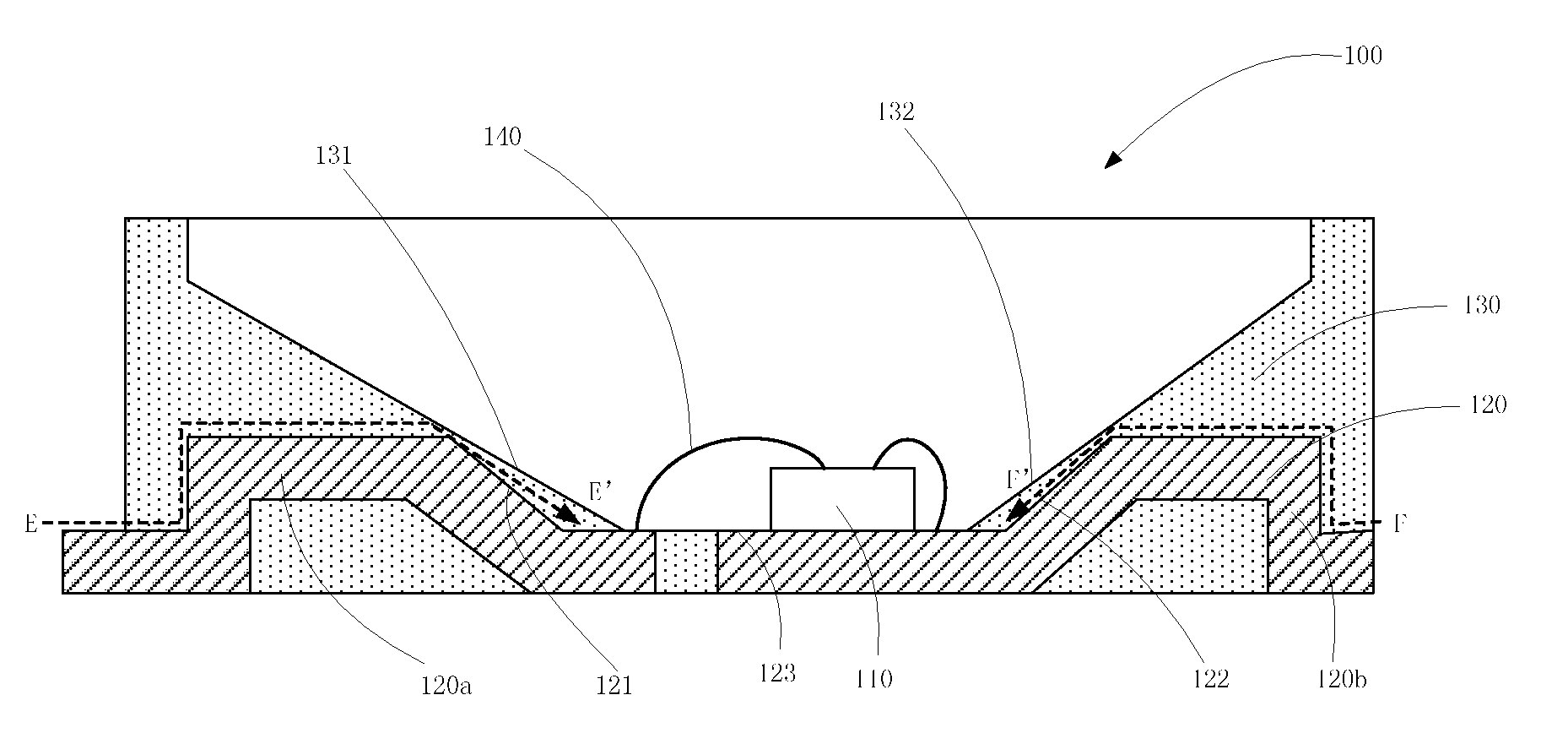
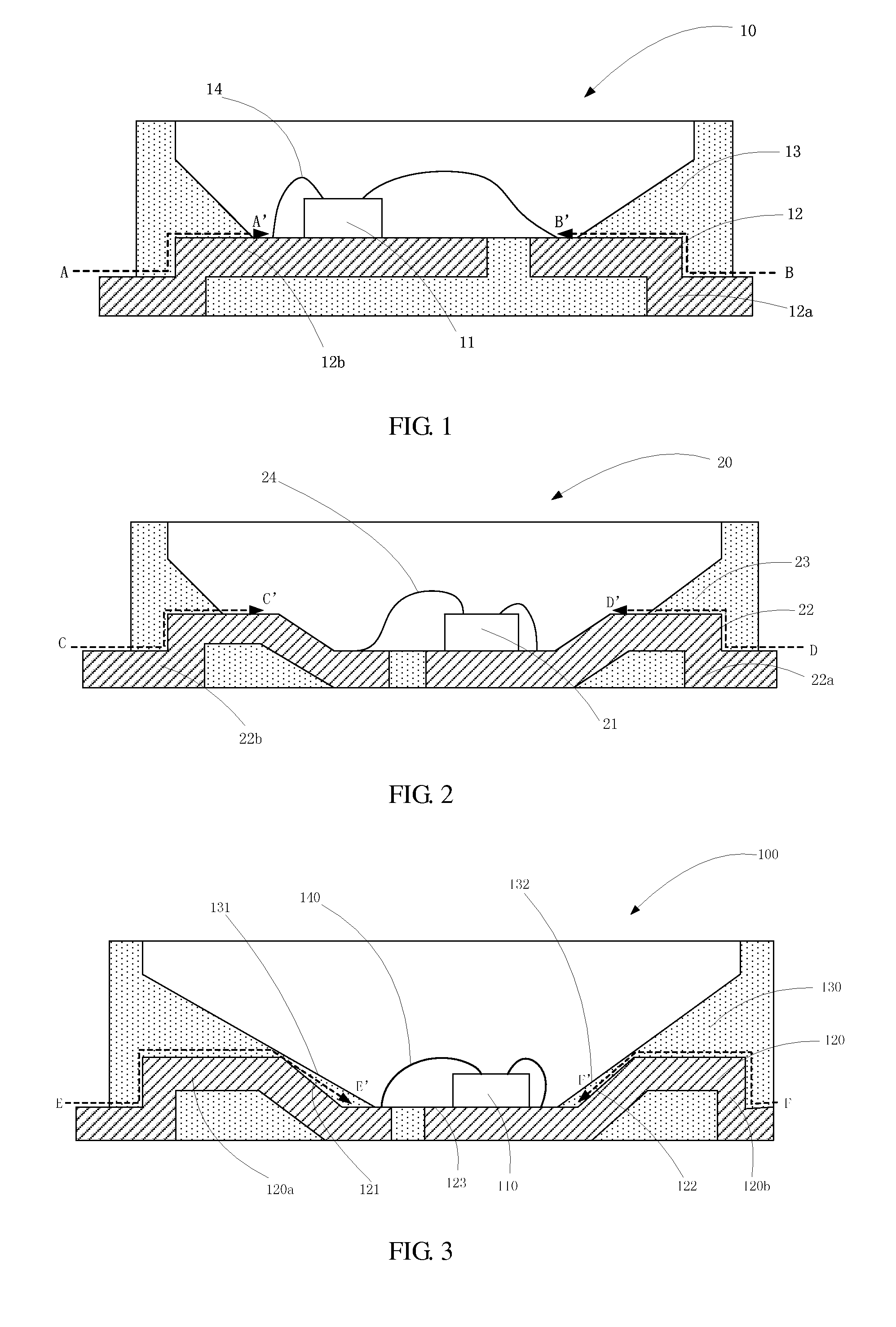
[0033]The technical method for realizing the invention purpose will be illustrated in detail by integrating the attached drawings and the exemplary embodiments. It should be understood that the described exemplary embodiments herein are only used for illustrating this invention rather than limiting.

[0034]Referring to FIG. 3, an LED packaging structure 100 includes a casing 130, a lead frame 120 arranged in the casing 130, an LED chip 110 located on a surface of the lead frame 120, and a transparent resin (not shown in the FIG). The lead frame 120 includes a first metal electrode 120a and a second metal electrode 120b. Said first metal electrode 120a and said second metal electrode 120b are disconnected from each other and connected to a positive electrode and a negative electrode of an external power supply (not shown in the FIG), respectively. The first metal electrode 120a and the second metal electrode 120b are electrically connected with a positive electrode and a negative elect...


PUM


Abstract

An LED packaging structure includes a casing, an LED chip, and a lead frame arranged in the casing, The lead frame includes a bottom portion, and a first metal side wall and a second metal side wall respectively located on two sides of said bottom portion. The LED chip is arranged on the bottom portion. Plastic layers with high reflectivity are respectively disposed on surfaces of the first metal side wall and the second metal side wall are provided with and are extended towards the direction far away from the bottom portion and joint with the casing. The LED packaging structure of the present disclosure not only provides a longer path for the moisture to permeate the inside of the LED packaging structure, but also reduces the loss of the luminous flux due to light emitted from the LED chip irradiating on the metal bracket.

Description

BACKGROUND[0001]1. Technical Field[0002]The present disclosure relates to the field of liquid crystal display, in particular to an LED packaging structure of a backlight module.[0003]2. Description of Related Art[0004]LED (Light Emitting Diode) is a common light source, which has the advantages of low power consumption, long service life, etc. Thus, LEDS are widely applied to the fields of lighting and liquid crystal display etc. Wherein, the LED packaging structure exerts profound significance for improving the light emission and heat dissipation.[0005]As is shown in FIG. 1, which is the schematic diagram showing the LED packaging structure with the lead frame having the plane structure in the prior art. The LED packaging structure 10 includes a casing 13, a lead frame 12 arranged in the casing 13 and an LED chip 11 located on a surface of the lead frame 12. The lead frame 12 includes two metal electrodes 12a and 12b disconnected from each other, and the LED chip 11 is arranged on ...

Claims


Application Information

Patent Timeline
IPC IPC(8): G02F1/1335H01L33/60
CPCH01L33/486H01L33/60H01L33/62H01L2924/0002H01L2924/00H01L2224/48091H01L2224/48247H01L2224/48257H01L2924/00014
Inventor CHANG, KUANG-YAOZHENG, WEIWEI
Owner TCL CHINA STAR OPTOELECTRONICS TECH CO LTD
Why Eureka
Try Eureka