Contact structure and method of manufacturing contact structure

Inactive Publication Date: 2013-02-07
TOKYO ELECTRON LTD
View PDF6 Cites 3 Cited by
  • Summary
  • Abstract
  • Description
  • Claims
  • Application Information

AI Technical Summary

Benefits of technology

[0012]According to the present invention, because the coat film of the housing acts as an electric current path, and the probe and the housing which are required to have elasticity are configured as separate bodies, the degree of flexibility in selecting the mater

Problems solved by technology

For example, with miniaturization of device electrodes, it is necessary to make needles physically small in size, bu

Method used


Image

  • Contact structure and method of manufacturing contact structure
  • Contact structure and method of manufacturing contact structure
  • Contact structure and method of manufacturing contact structure

Examples


Embodiment Construction

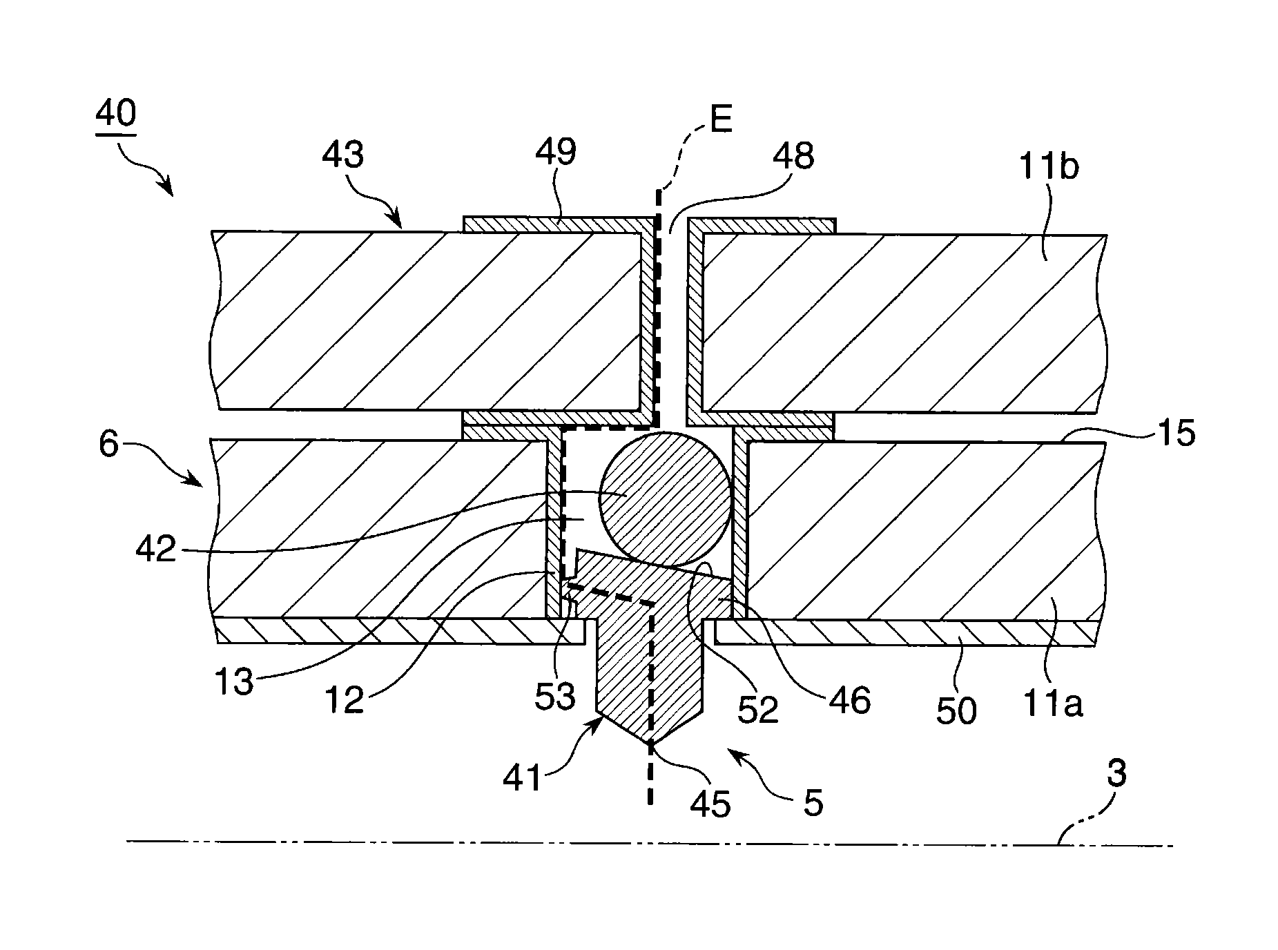
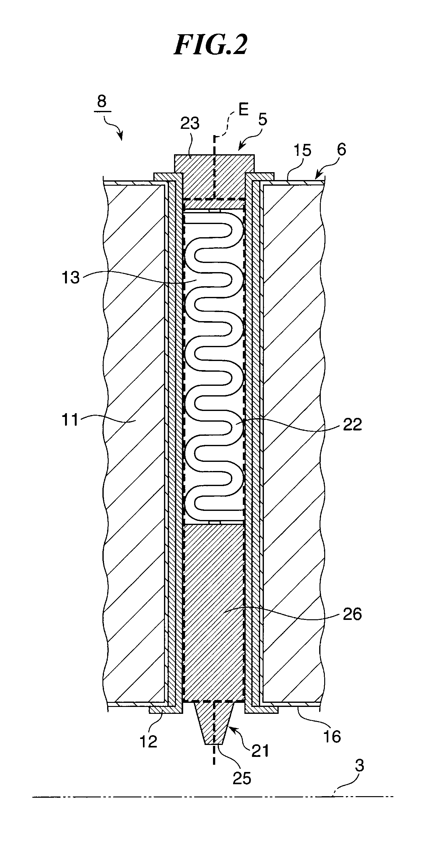
[0022]Embodiments of the present invention will now be described with reference to the drawings. It should be noted that in the present specification and the drawings, elements having substantially the same functional arrangements are designated by the same reference symbols, and duplicate description thereof is omitted.

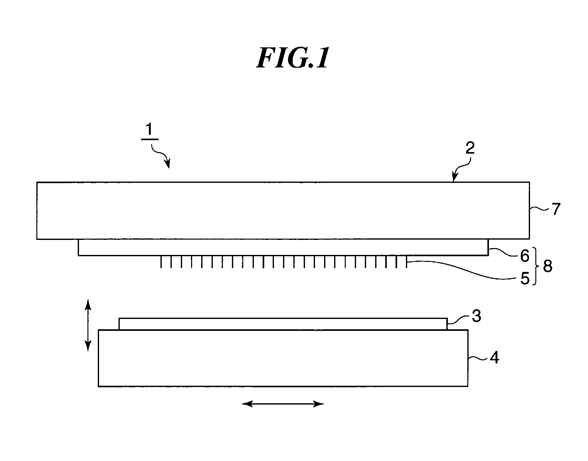
[0023]FIG. 1 is a side view schematically showing an arrangement of a probe unit 1 for which a contact structure according to the present invention is used. The probe unit 1 is equipped with, for example, a probe card 2, and a mounting stage 4 on which a subject to be inspected 3 such as a wafer is mounted. The mounting stage 4 is movable vertically and horizontally. The probe card 2 has, for example, a plurality of probes 5, a housing 6 that supports the probes 5, and a circuit board 7 that sends and receives electric signals to and from the probes 5. The housing 6 is, for example, disk-shaped and opposed to the mounting stage 4 below. It should be noted that in the...


PUM

PropertyMeasurementUnit
Electrical conductoraaaaaaaaaa
Circumferenceaaaaaaaaaa
Elasticityaaaaaaaaaa

Abstract

A contact structure has a probe and a housing disposed on an outer circumference thereof. The housing has a housing main body in which a hollow section vertically penetrating the same is formed, and a conductive coat film with which an inner wall surface of the hollow section is coated. The probe has a base end portion fixed in place on one end side of the housing, a conductive leading end portion that is movable in the hollow section while being in contact with the coat film and has, on a leading end thereof, a contact that comes into contact with a subject to be inspected, and an elastic portion that connects together the base end portion and the leading end portion, is disposed in the hollow section, and has elasticity.

Description

TECHNICAL FIELD[0001]The present invention relates to a contact structure, which comes into contact with a subject to be inspected so as to inspect electrical characteristics of the subject to be inspected, and a method of manufacturing the contact structure.BACKGROUND ART[0002]Electrical characteristics of an electronic circuit such as an IC or an LSI formed on a semiconductor wafer (hereafter referred as a “wafer”) are usually inspected using a probe unit. The probe unit is constructed such that multiple probes are supported on a lower surface of a probe card. Electrical characteristics of a wafer are inspected by bringing leading ends of the multiple probes into a plurality of electrodes in the electronic circuit, and sending and receiving electric signals between needles and the electrodes.[0003]In this inspection, needles for transmitting electric signals supplied from a tester are temporarily brought into contact with fine electrodes formed on a semiconductor device. The needl...

Claims


Application Information

Patent Timeline
IPC IPC(8): G01R1/067C25D1/00
CPCG01R1/06722G01R3/00G01R1/067H01L22/00
Inventor SATO, YOHEIHOSHINO, TOMOHISA
Owner TOKYO ELECTRON LTD
Why Eureka
Try Eureka