Touch-sensing panel and touch-sensing display apparatus
a touch sensor and display device technology, applied in the field of touch sensors, can solve the problems of reducing the whole qualitative reducing the flexibility of circuit layout and fabrication etc., and achieves the effect of improving the design sense of the touch sensor panel and increasing the flexibility of circuit layout and fabrication
- Summary
- Abstract
- Description
- Claims
- Application Information
AI Technical Summary
Benefits of technology
Problems solved by technology
Method used
Image
Examples
first embodiment
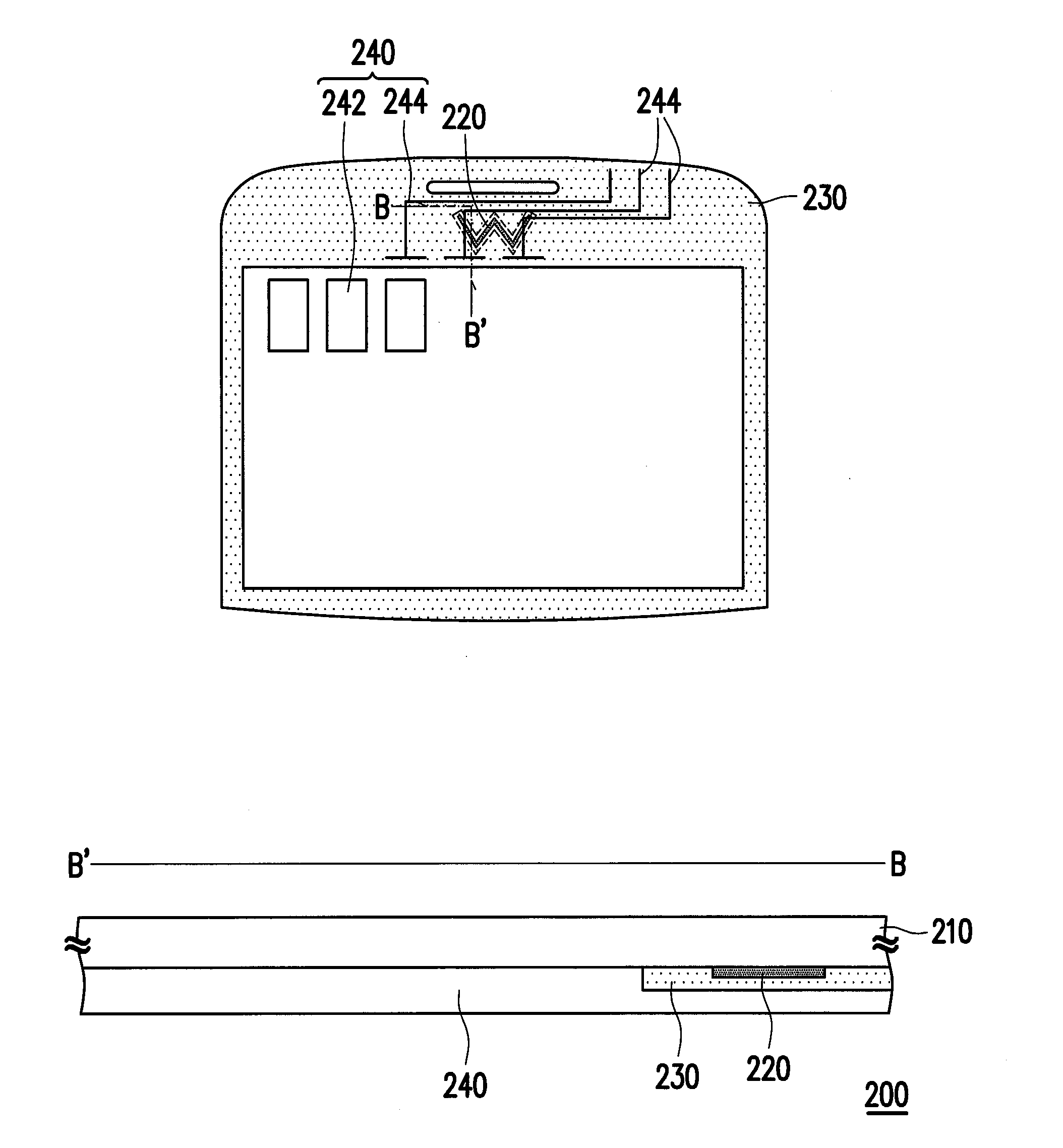
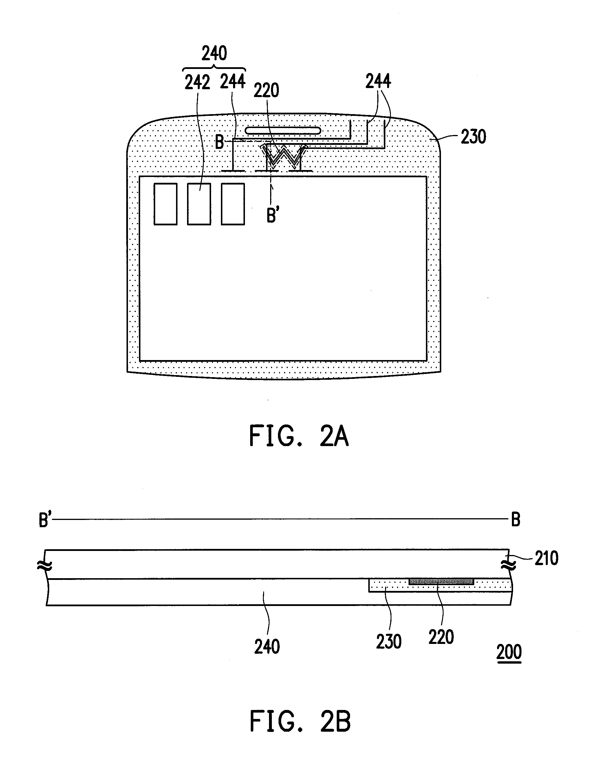
[0024]Referring to FIG. 2A and FIG. 2B, FIG. 2B is a cross-sectional view of FIG. 2A along a section line BB′. A touch-sensing panel 200 includes a substrate 210, a logo pattern 220, a decoration layer 230 and a touch-sensing element 240. The touch-sensing element 240 is disposed on the substrate 210. In the embodiment, the touch-sensing element 240 includes at least one touch-sensing unit 242 and at least one transmission line 244 electrically connected to the touch-sensing unit 242. The logo pattern 220 is disposed at a predetermined position on the substrate 210, and a designer can present a brand logo, a key icon or any desired figure on such region through the logo pattern 220. The decoration layer 230 is disposed on surface periphery of the substrate 210.
[0025]The decoration layer 230 of the present embodiment wraps the logo pattern 220 on the substrate 210, so that the logo pattern 220 is not exposed to the outside to cause oxidation, and decrease of qualitative sense thereof...
second embodiment
[0032]Referring to FIG. 5, a touch-sensing panel 300 of the present embodiment is similar to the touch-sensing panel 200 of the first embodiment, and the same components are denoted by the same symbols. Though, compared to the touch-sensing panel 200 of the first embodiment, the touch-sensing panel 300 of the present embodiment further has a color matching layer 310.
[0033]In order to further increase a special visual variation of the logo pattern 220 to achieve an optimal visual effect, the color matching layer 310 is disposed on the logo pattern 220. A material of the color matching layer 310 can be photoresist of different colors, ceramic, ink or diamond-like carbon, etc. according to an actual product design or color matching requirement, for example, a red filter photoresist, a blue filter photoresist or a green filter photoresist of a color filter layer. As a color of the color matching layer 310 is different to a color of the decoration layer 230, the logo pattern 220 may pres...
PUM
 Abstract
Description
Claims
Application Information


