Touch panel

a technology of touch panel and touch screen, which is applied in the field of touch panel, can solve the problems of reducing the supply of materials, reducing the efficiency of product driving, and increasing the consumption of materials in the futur

Inactive Publication Date: 2013-03-14
SAMSUNG ELECTRO MECHANICS CO LTD
View PDF3 Cites 161 Cited by
  • Summary
  • Abstract
  • Description
  • Claims
  • Application Information

AI Technical Summary

Benefits of technology

[0010]The present invention has been made in an effort to provide a touch panel capable of solving a depletion problem of resources used for a transparent conductive layer, in particular, improving a moiré phenomenon occurring during a image projection process when a metal electrode in a mesh shape is formed to have two layers, by replacing ITO and forming electrodes using a metal thin film on which fine patterns are formed.

Problems solved by technology

It is difficult to efficiently drive products only by the keyboard and the mouse serving as the present input devices.
When considering the rising demand for applications due to excellent characteristics of the ITO as a transparent electrode, it is expected that the consumption of the material is gradually increased in the future.
However, indium forming ITO is a representative one of scarce and depleting resources and the supply thereof is greatly reduced.
The indium needs to be purified using by-products of a zinc ore, which also leads to high scarcity.
Even before the indium is depleted, the sudden rise in indium price leads to increase manufacturing costs of applications.

Method used


Image

  • Touch panel
  • Touch panel
  • Touch panel

Examples


first preferred embodiment

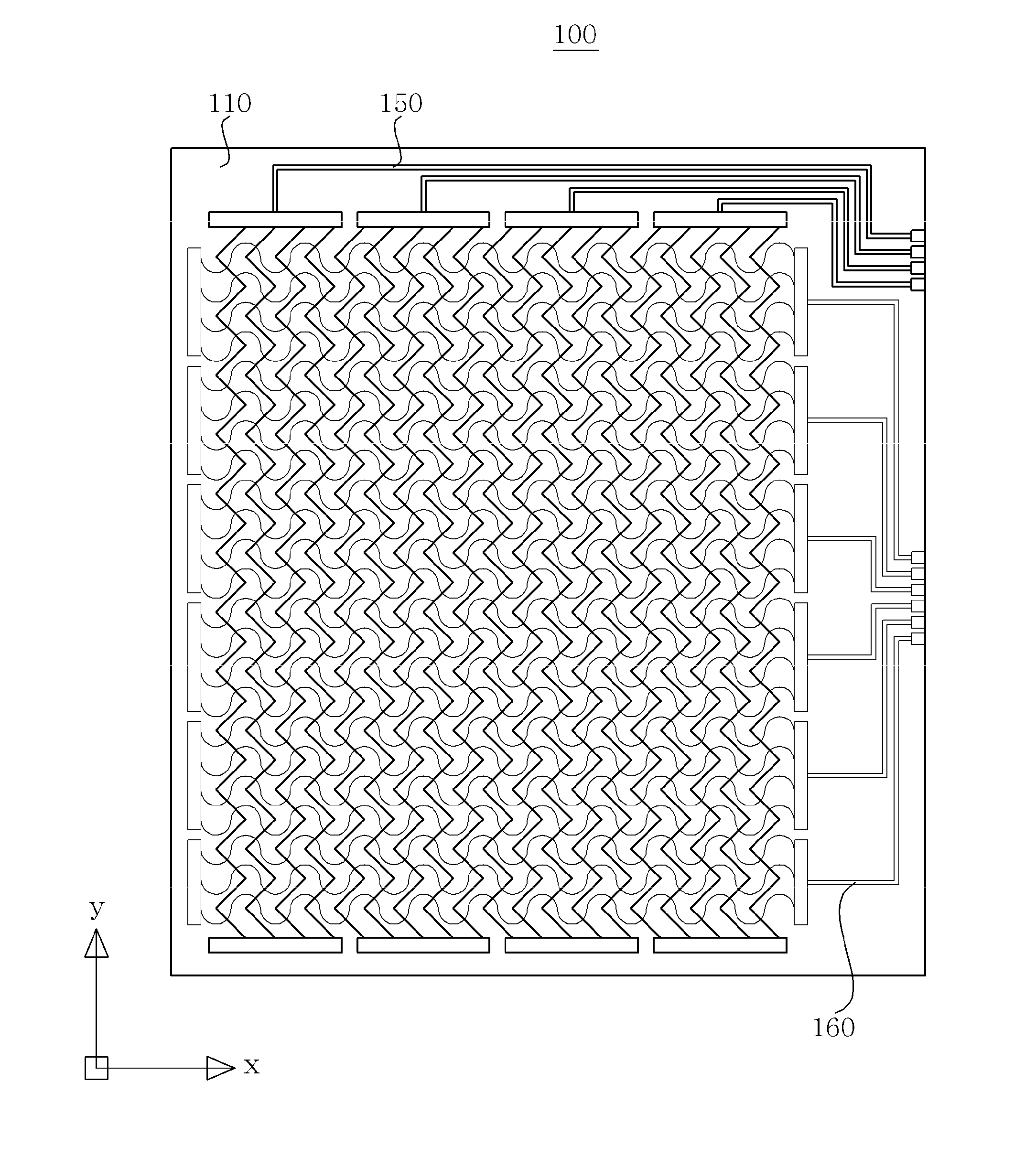
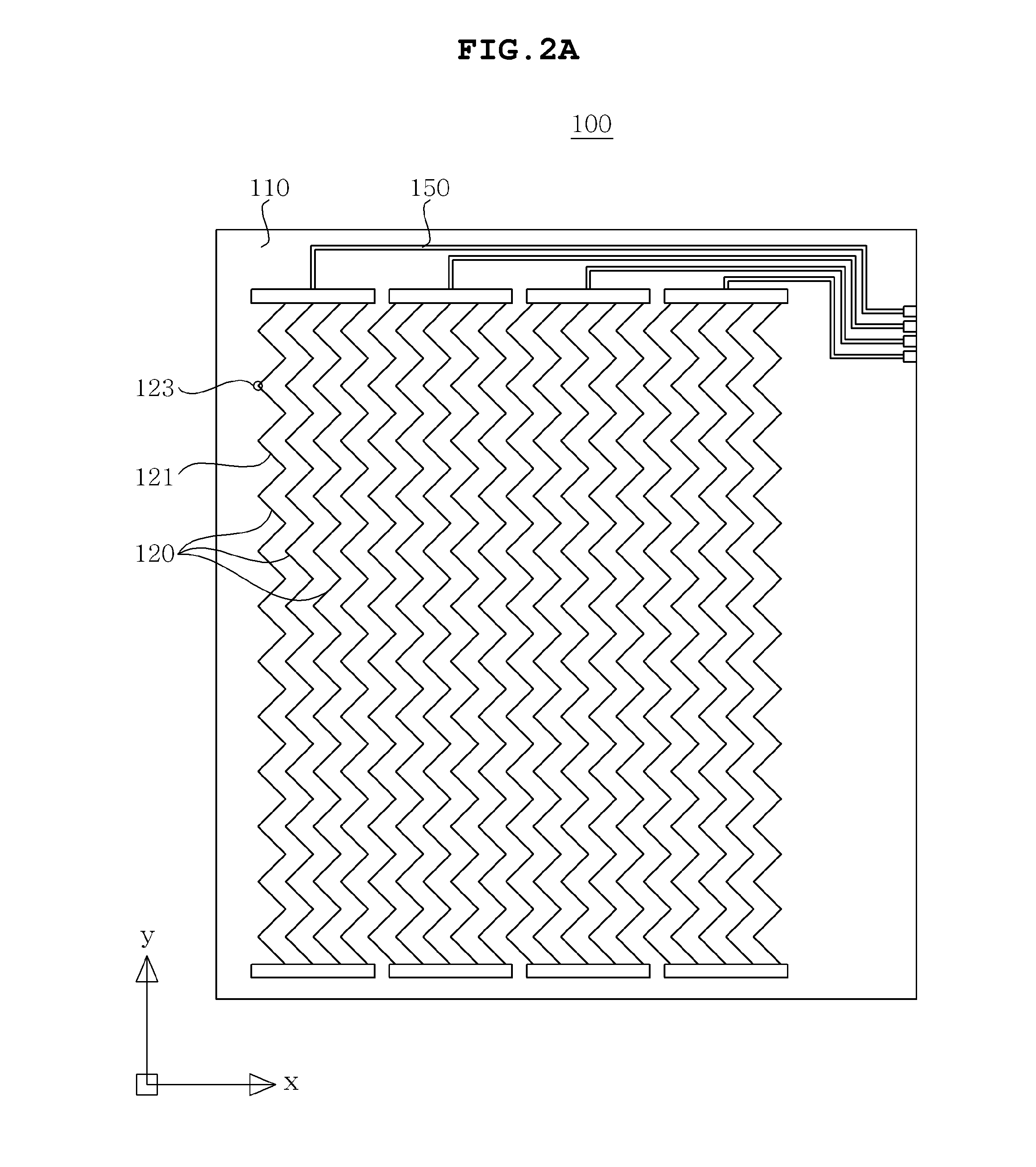
[0044]FIG. 1 is a plan view of the touch panel according to a first preferred embodiment of the present invention. As shown in FIG. 1, a touch panel 100 according to the preferred embodiment of the present invention is configured to include a transparent substrate 110 and a first metal electrode 120 and a second metal electrode 130 each formed on both surfaces of the transparent substrate 110.

[0045]The transparent substrate 110 serves to provide a region in which the metal electrodes 120 and 130 (see FIG. 2) and electrode wirings 150 and 160 are formed. In this configuration, the transparent substrate 110 is partitioned into an active region and a bezel region, wherein the active region is a portion in which the metal electrodes 120 and 130 are formed so as to recognize a touch of an input unit and is disposed at a center of the transparent substrate 110 and the bezel region is a portion in which the electrode wirings 150 and 160 extending from the metal electrodes 120 and 130 are f...

second preferred embodiment

[0077]Meanwhile, FIG. 3A is a perspective view of a touch panel according to a second preferred embodiment of the present invention and FIG. 3B is a cross-sectional view of the touch panel according to the preferred embodiment of the present invention. As shown in FIG. 3B, the touch panel according to the second preferred embodiment of the present invention may be formed by bonding front surfaces of a pair of transparent substrates 210 and 260 having metal electrodes 220 and 230 formed on surfaces thereof by an adhesive 280. That is, the first metal electrode 220 is formed on one surface of the first transparent substrate 210 and the second metal electrode 230 is formed on one surface of the second transparent substrate 260 and the adhesive280 is generally formed between one surface of the first transparent substrate 210 and one surface of the second transparent substrate 260 to bond the front surfaces of both transparent substrates, thereby forming the touch panel 200. The adhesive...

third preferred embodiment

[0083]FIGS. 4 and 5 are plan views of a touch panel according to a third preferred embodiment of the present invention. A first metal electrode 320 is formed on one surface of a transparent substrate 310 (see FIG. 5A) and a second metal electrode 330 is formed on the other surface of the transparent substrate 310(see FIG. 5B). In addition, a first electrode wiring 350 is formed on one surface of the transparent substrate 310 so as to extend from one end of the first metal electrode 320 and a second electrode wiring 360 is formed on the other surface of the transparent substrate 310 so as to extend from one end of the second metal electrode 330.

[0084]The detailed description of the transparent substrate 31Q and the electrode wirings 350 and 360 is the same as one described in the first preferred embodiment and the repeated description thereof will be omitted. Hereinafter, the shape of the first metal electrode 320 and the second metal electrode 330 will be described in detail.

[0085]F...


PUM

PropertyMeasurementUnit
interior angleaaaaaaaaaa
widthaaaaaaaaaa
widthaaaaaaaaaa

Abstract

Disclosed herein is a structure of a touch panel capable of solving a depletion problem of resources used for a transparent conductive layer, in particular, improving a moiré phenomenon occurring during a image projection process when a metal electrode in a mesh shape is formed on both surfaces of the transparent substrate, by replacing ITO and forming electrodes using a metal thin film on which fine patterns are formed. Exemplary embodiments of the present invention can improve the moiré phenomenon occurring due to overlapping lines between the top and bottom metal electrodes on the transparent substrate during the image projection process and can improve the visibility by minimizing overlapping lines between the metal electrode formed on the transparent substrate and the pixel grid or the black matrix formed on the color filter.

Description

CROSS REFERENCE TO RELATED APPLICATION[0001]This application claims the benefit of Korean Patent Application No. 10-2011-0091155, filed on Sep. 8, 2011, entitled “Touch Panel”, which is hereby incorporated by reference in its entirety into this application.BACKGROUND OF THE INVENTION[0002]1. Technical Field[0003]The present invention relates to a touch panel.[0004]2. Description of the Related Art[0005]As a computer using a digital technology is developed, accessory devices of the computer have also been developed. A personal computer, a portable transmission device, and other personal only information processing devices, or the like, perform text and graphic processing using various input devices such as a keyboard, a mouse, or the like.[0006]However, as an information-oriented society is rapidly progressed, a usage of the computer has gradually expanded. It is difficult to efficiently drive products only by the keyboard and the mouse serving as the present input devices. Therefore...

Claims


Application Information

Patent Timeline
Patent Type & Authority Applications(United States)
IPC IPC(8): G06F3/041
CPCG06F3/0412G06F2203/04112G06F3/0445G06F3/0446G06F2203/04103
Inventor LEE, WOO JINKIM, JAE HUNYANG, CHUNG MOLEE, IN HYUNGHONG, SANG SULEE, YOUNG WOO
Owner SAMSUNG ELECTRO MECHANICS CO LTD
Why Eureka
Try Eureka