Dual metal integration scheme based on full silicidation of the gate electrode

Inactive Publication Date: 2007-10-04
IBM CORP
View PDF6 Cites 17 Cited by
  • Summary
  • Abstract
  • Description
  • Claims
  • Application Information

AI Technical Summary

Benefits of technology

[0009] The present application provides an integration scheme that enables full silicidation (FUSI) of the gate electrodes at the same time as that of the source / drain regions. The FUSI of the gate electrodes eliminates the gate depletion problem that is observed with polysilicon gate electrodes. In addition, the inventive integration scheme creates different silicon thicknesses of the gate electrode just prior to silicidation. This feature of the present invention allows for fabricating nFETs and pFETs that have an essential band edge workfunction that is tailored for the specific device region. By “essential band edge workfunction” it is meant a workfunction that is about 200 meV or less from the band edge.

Problems solved by technology

One disadvantage of utilizing polysilicon gates is that at inversion, the polysilicon gates generally experience depletion of carriers in the area of the polysilicon gate that is adjacent to the gate dielectric.
The depletion effect reduces the effective gate capacitance of the MOSFET.
The decrease in resistance causes a decrease in the time propagation delay RC of the gate.
Although a silicide top gate region may help decrease the resistance of the transistor, charge is still depleted in the vicinity of the interface formed between the bottom polysilicon gate and gate dielectric, thereby causing a smaller effective gate capacitance.
This prevents the increase in effective thickness of the gate capacitor and the capacitance increases as a result of the depletion effect.
Although metal gates can be used to eliminate the poly-depletion effect and to provide lower gate resistance, it is generally quite difficult to offer multiple-threshold voltages with metal gates.
That is, it is difficult to tailor metal gate stacks such that the workfunction thereof meets a desired value for application in a specific device area.

Method used


Image

  • Dual metal integration scheme based on full silicidation of the gate electrode
  • Dual metal integration scheme based on full silicidation of the gate electrode
  • Dual metal integration scheme based on full silicidation of the gate electrode

Examples


Embodiment Construction

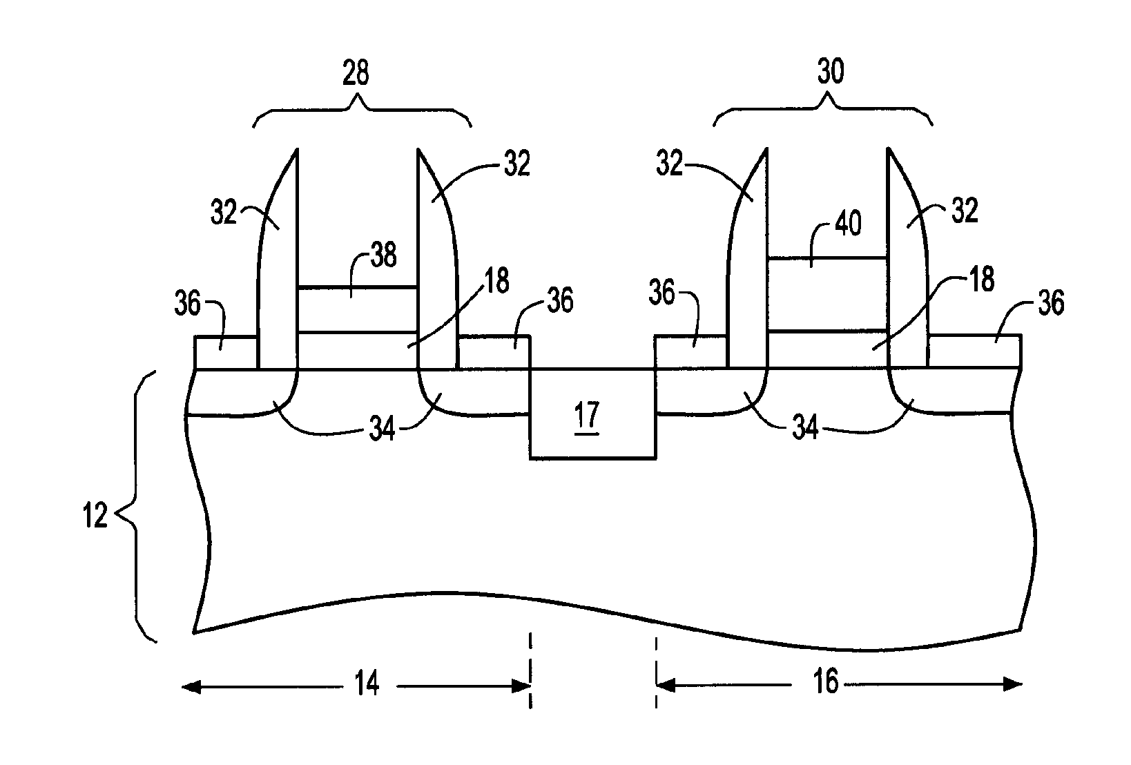
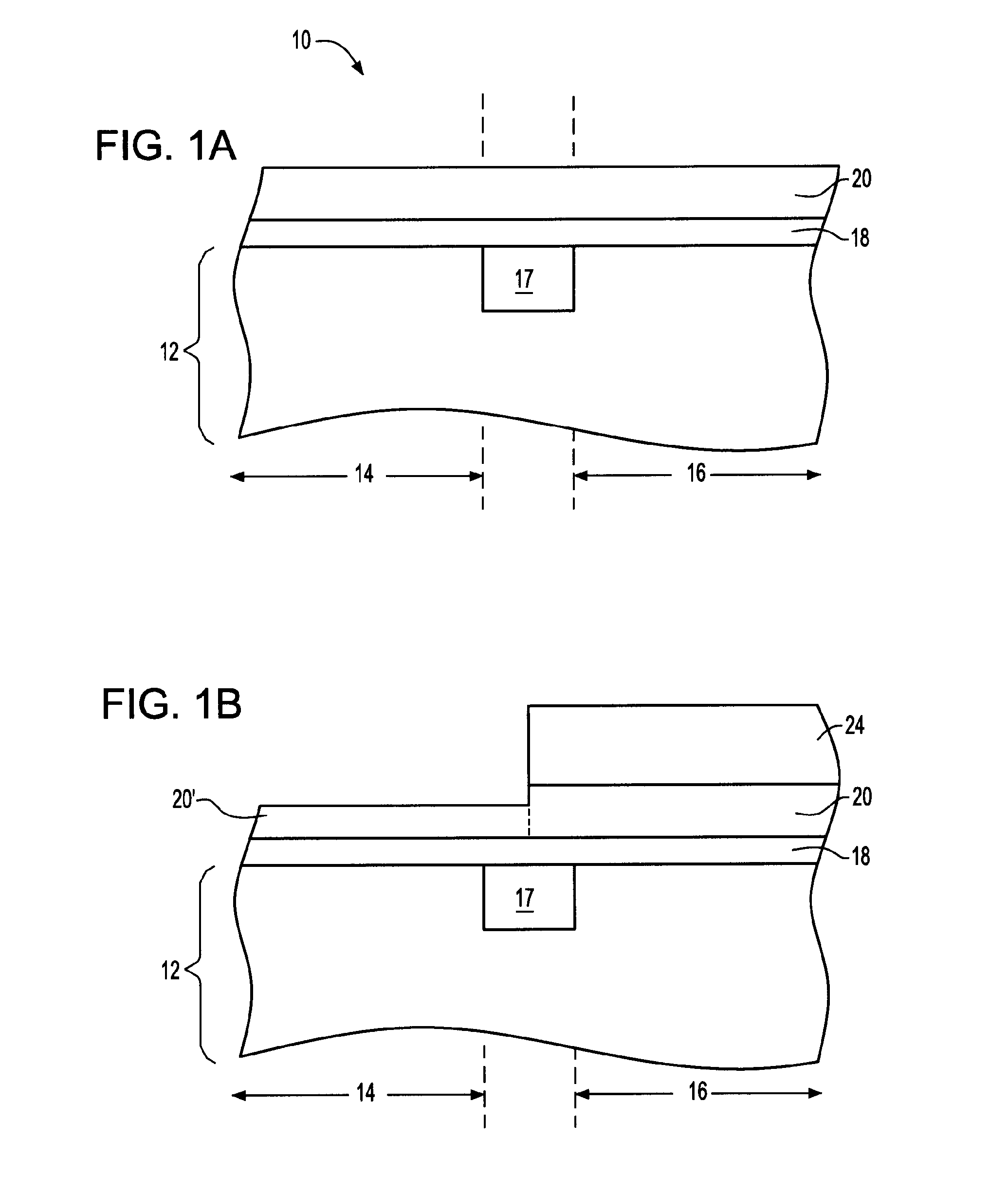
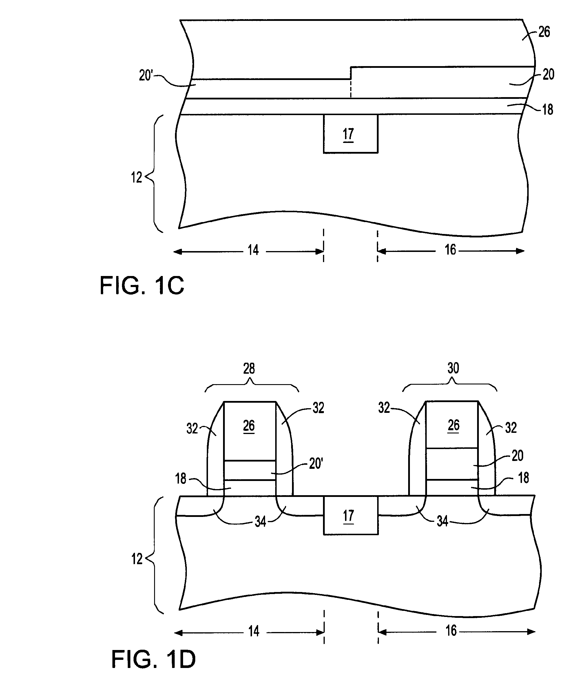
[0019] The present invention, which provides a dual metal integration scheme for fabricating fully silicided gate electrodes having workfunctions tailored for a specific device region, will now be described in greater detail by referring to the following discussion and drawings that accompany the present application. The drawings of the present application, which are referred to herein below in greater detail, are provided for illustrative purposes and, as such, they are not drawn to scale.

[0020] In the following description, numerous specific details are set forth, such as particular structures, components, materials, dimensions, processing steps and techniques, in order to provide a thorough understanding of the present invention. However, it will be appreciated by one of ordinary skill in the art that the invention may be practiced without these specific details. In other instances, well-known structures or processing steps have not been described in detail in order to avoid obs...


PUM


Abstract

An integration scheme that enables full silicidation (FUSI) of the nFET and pFET gate electrodes at the same time as that of the source / drain regions is provided. The FUSI of the gate electrodes eliminates the gate depletion problem that is observed with polysilicon gate electrodes. In addition, the inventive integration scheme creates different silicon thicknesses of the gate electrode just prior to silicidation. This feature of the present invention allows for fabricating nFETs and pFETs that have a band edge workfunction that is tailored for the specific device region.

Description

FIELD OF THE INVENTION [0001] The present invention relates to a semiconductor structure and a method of fabricating the same. More specifically, the present invention provides a semiconductor structure including a fully silicided nFET gate electrode and a fully silicided pFET gate electrode integrated on the same semiconductor substrate and a method of fabricating the same. BACKGROUND OF THE INVENTION [0002] In current metal oxide semiconductor field effect transistors (MOSFETs), a polysilicon gate is typically employed. One disadvantage of utilizing polysilicon gates is that at inversion, the polysilicon gates generally experience depletion of carriers in the area of the polysilicon gate that is adjacent to the gate dielectric. This depletion of carriers is referred to in the art as the polysilicon depletion effect. The depletion effect reduces the effective gate capacitance of the MOSFET. Ideally, it is desirable that the gate capacitance of the MOSFET be high since high gate cap...

Claims


Application Information

Patent Timeline
IPC IPC(8): H01L21/8234
CPCH01L21/823443H01L21/823842H01L21/823835H01L21/82345
Inventor HENSON, WILLIAM K.RIM, KERNMANDELMAN, JACK A.
Owner IBM CORP
Why Eureka
Try Eureka