System and memory module
a memory module and system technology, applied in the field of memory modules, can solve the problems of signal quality degradation caused by a stub, signal quality degradation, and the size of a so-called data eye decreases, and achieve the effect of high signal quality
- Summary
- Abstract
- Description
- Claims
- Application Information
AI Technical Summary
Benefits of technology
Problems solved by technology
Method used
Image

Examples
first exemplary embodiment
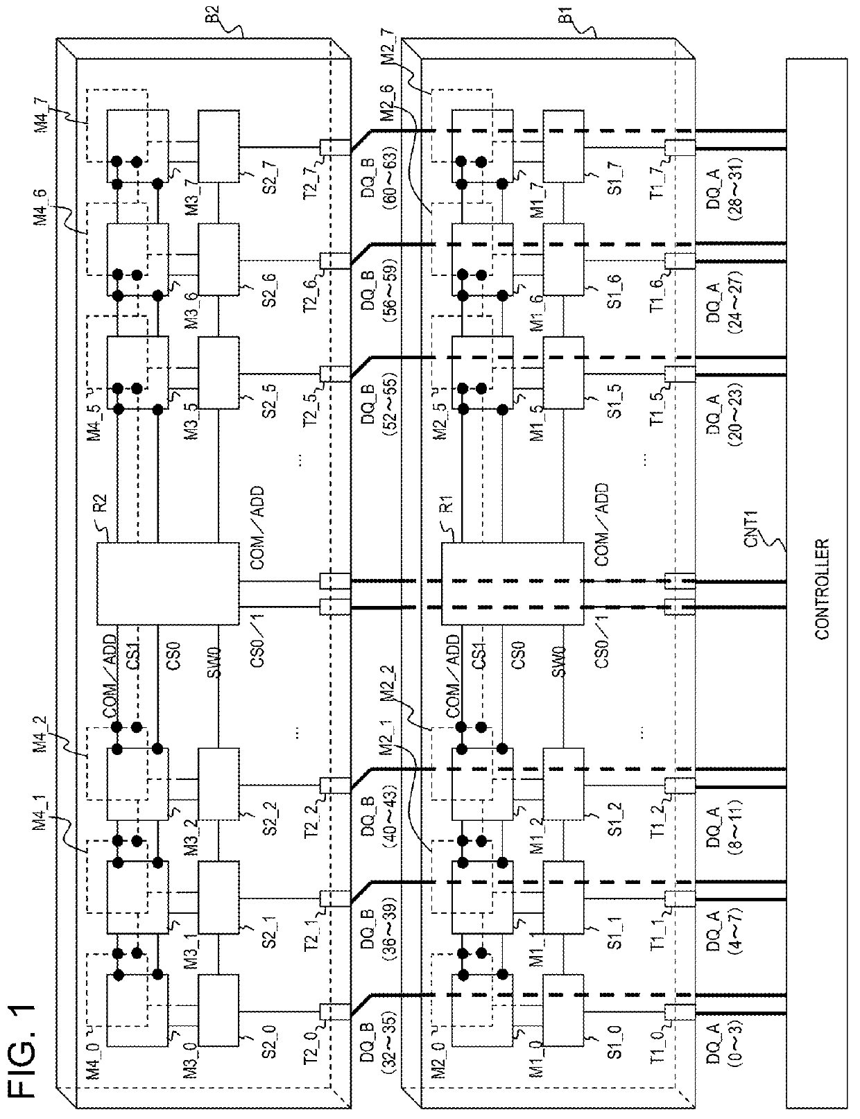
[0044]A system according to a first exemplary embodiment will be described with reference to the drawings. FIG. 1 is a diagram showing, as an example, a configuration of the system according to the present exemplary embodiment. FIG. 1 is a plan view of the whole of the system. Module substrates are stereoscopically displayed in order to easily see the configuration.
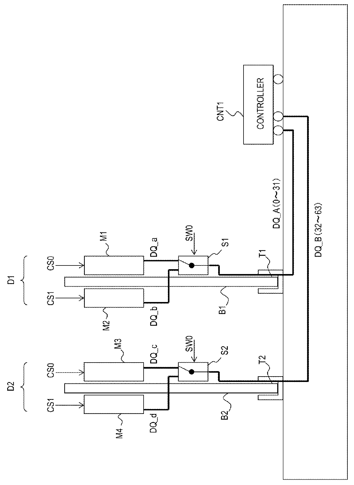
[0045]Referring to FIG. 1, the system in the present exemplary embodiment includes a controller CNT1 and two memory modules. A first memory module includes memory chips M1_0 to M1_7, data terminals T1_0 to T1_7, switch units S1_0 to S1_7, and a register R1 on the front surface of a module substrate B1. The first memory module includes memory chips M2_0 to M2_7 on the back surface of the module substrate B1. Similarly, a second memory module includes memory chips M3_0 to M3_7, data terminals T2_0 to T2_7, switch units S2_0 to S2_7, and a register R2 on the front surface of a module substrate B2. The second module includes ...
second exemplary embodiment
[0065]A system according to a second exemplary embodiment will be described, with reference to the drawings. FIG. 4 is a diagram showing a configuration of the system according to the present exemplary embodiment. The system in the present exemplary embodiment is different from the system in the first exemplary embodiment in that 64 data buses are provided for each memory module. The memory module included in the system in the present exemplary embodiment can be used in the system shown in FIG. 9 as the related art, as well.
[0066]Referring to FIG. 4, in the system in the present exemplary embodiment, a memory module D1 includes a switch unit SX1. On the other hand, a memory module D2 includes a switch unit SX2. In the system in the present exemplary embodiment, a cross-bus switch is used for each of the switch units SX1 and SX2. In this case, 32 data terminals T1 and 32 data terminals T11 are provided on both front and back surfaces of a module substrate B1 of the memory module D1, ...
third exemplary embodiment
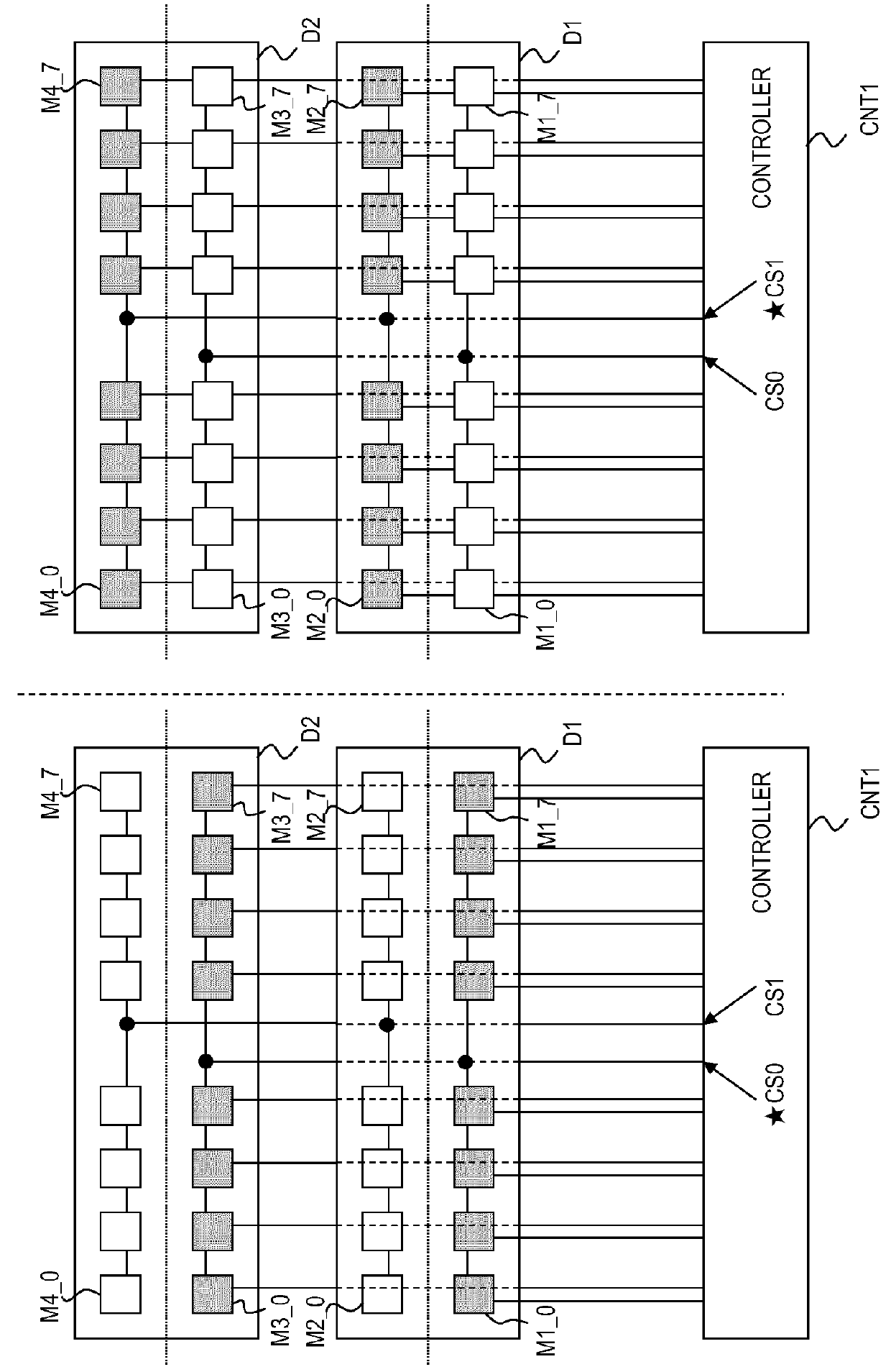
[0070]A system according to a third exemplary embodiment will be described, with reference to the drawings. FIG. 6 is a diagram showing, as an example, a configuration of the system in the present exemplary embodiment. In the first exemplary embodiment (in FIG. 1), one switch unit (including a buffer circuit) is provided for a set of memory chips on the front and back surfaces of each memory module. On the other hand, one switch unit (including a switch circuit / buffer circuit for two chips) is provided for two sets of memory chips on the front and back surfaces of each memory module, for example.
[0071]Referring to FIG. 6, one switch unit SL0 is provided for memory chips M1_0 and M1_1 on the front surface of a module substrate B1 and memory chips M2_0 and M2_1 on the back surface of the module substrate B1. Similarly, one switch unit SL1 is provided for memory chips M1_6 and M1_7 on the front surface of the module substrate B1 and memory chips M2_6 and M2_7 on the back surface of the...
PUM
 Abstract
Description
Claims
Application Information
 - Generate Ideas
- Intellectual Property
- Life Sciences
- Materials
- Tech Scout
- Unparalleled Data Quality
- Higher Quality Content
- 60% Fewer Hallucinations
Browse by: Latest US Patents, China's latest patents, Technical Efficacy Thesaurus, Application Domain, Technology Topic, Popular Technical Reports.
© 2025 PatSnap. All rights reserved.Legal|Privacy policy|Modern Slavery Act Transparency Statement|Sitemap|About US| Contact US: help@patsnap.com