Imaging device

a technology of imaging device and image, which is applied in the field of imaging device, can solve the problems of image interference, more significant image interference, and the likely subject of the imaging device to electromagnetic interference, so as to prevent the tilting of the imaging element, reduce the image interference caused by an external noise, and prevent the tilting of the metal plate

Inactive Publication Date: 2013-03-28
PANASONIC CORP
View PDF9 Cites 8 Cited by
  • Summary
  • Abstract
  • Description
  • Claims
  • Application Information

AI Technical Summary

Benefits of technology

[0016]As described above, in the imaging device of the present disclosure, a load point of the electrically-conductive component is positioned in the load positioning area surrounded by three fixing points on the metal plate, thereby applying a load from the electrically-conductive component to the metal plate in a balanced manner. Therefore, tilting of the metal plate is prevented and tilting of the imaging element can be prevented. Therefore, also when the imaging device is used in an intense electric field environment, image interference caused by an external noise can be reduced while preventing the imaging element from tilting. These and other objects, features, aspects and advantages of the present disclosure will become more apparent from the following detailed description of the present disclosure when taken in conjunction with the accompanying drawings.

Problems solved by technology

In a case where the imaging device is used in such an environment, the imaging device is likely to be subjected to an electromagnetic interference.
Hereinafter, an environment in which imaging devices are likely to be subjected to such an electromagnetic interference is referred to as an “intense electric field environment.” If an imaging device such as a digital still camera is used in the intense electric field environment, an image taken by the imaging device may contain a stripe pattern noise (beat noise), and image interference may be caused.
The higher a performance of an imaging element of the imaging device is (the higher the sensitivity of an imaging element to be used is), the more significant the image interference is.
Further, in an imaging element built into an imaging device having been downsized as a result of the sizes of imaging devices being reduced, an amount of coupling of intense electric field noise from the outside is increased, so that the image interference becomes more significant.
Causes of the image interference include entering of an external electromagnetic wave into an image signal line of an imaging element.
However, in a case where, for example, an elastic component is provided at each fixing point in order to adjust the tilting of the metal surface, if the electrically-conductive component having been pressed against the back surface of the metal plate is inappropriately disposed, the metal plate may be tilted, which may cause the imaging element to be tilted.

Method used


Image

  • Imaging device
  • Imaging device
  • Imaging device

Examples


first embodiment

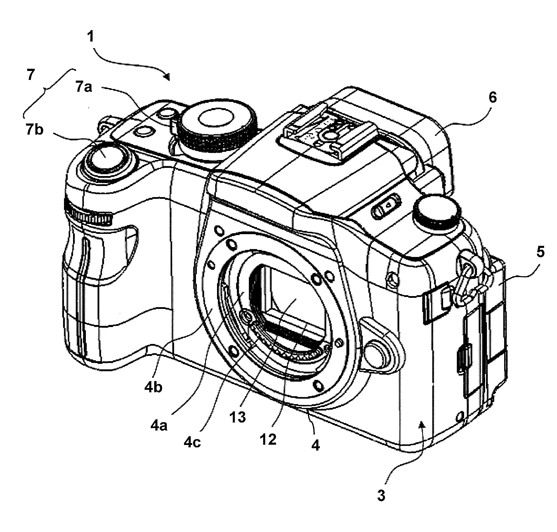
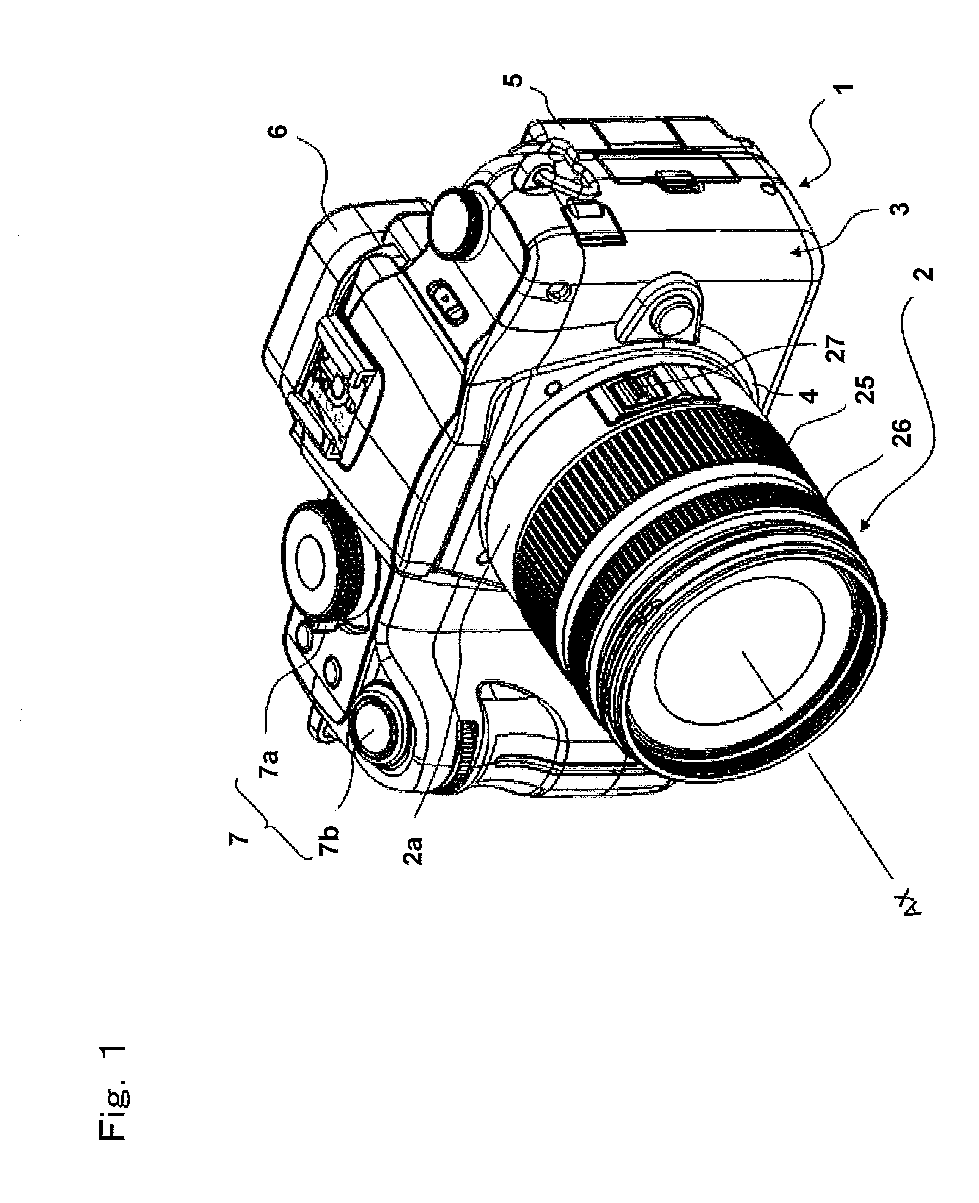
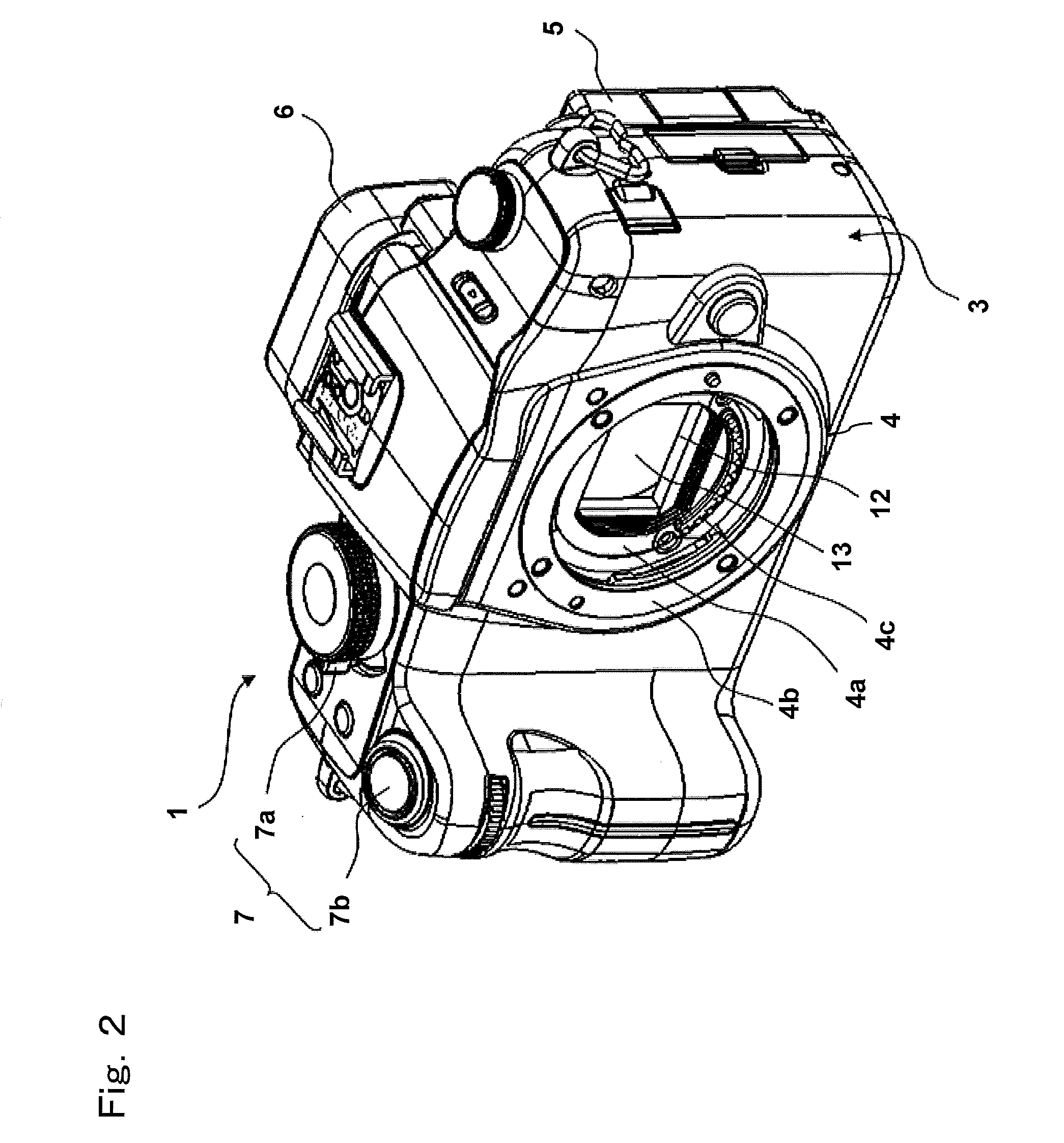
[0033]FIG. 1 is a perspective view illustrating an outer appearance of a digital camera (which is an exemplary imaging device) according to a first embodiment. The digital camera according to the first embodiment includes a camera main body 1 and an exchangeable lens unit 2 which is mountable to the camera main body 1. FIG. 2 is a perspective view of an outer appearance of the camera main body 1 from which the exchangeable lens unit 2 is removed. FIG. 3 is a schematic cross-sectional view of an internal structure of the digital camera. FIG. 4 is a functional block diagram illustrating the digital camera.

[0034]Firstly, referring to FIG. 1 to FIG. 4, a fundamental structure of the digital camera according to the first embodiment will be described. In the description herein, for convenience of description, an object side of the digital camera is referred to as the front, and an imaging plane side of the digital camera is referred to as the rear or the back.

[0035]As shown in FIG. 1, the...

second embodiment

[0087]FIG. 12 is a cross-sectional view illustrating an internal structure of an imaging device 200, as viewed from thereabove, according to a second embodiment. In description herein, difference from the first embodiment will be mainly described. A fundamental configuration of the imaging device 200 is the same as that of the digital camera described with reference to FIG. 1 to FIG. 4.

[0088]As shown in FIG. 12, the imaging device 200 includes the imaging element 110, the main circuit substrate 120, the imaging element flexible cable 130, the mount 140, the exchangeable lens mount section 145, the metal plate 150, the connection sections 160, the elastic components 165, and the electrically-conductive component 190. Further, the main circuit substrate 120 has the GND removal portion 180 and the AD conversion LSI 185 (an integrated circuit for AD conversion) on the front surface on the metal plate 150 side. In FIG. 12, the same components as described for the imaging device 100, as s...


PUM


Abstract

An imaging device 100 includes: an imaging element 110; a main circuit substrate 120; a mounting component 130 mounting the imaging element 110; a metal plate 150 disposed between the mounting component 130 and the main circuit substrate 120; a mount 140 supporting the metal plate 150 by connection sections 160 being fixed at at least three fixing points; elastic components 165 urging the connection sections 160 at each fixing point of the mount 140; and an electrically-conductive component 190 electrically connecting between a ground conductor of the main circuit substrate 120 and the metal plate 150. The electrically-conductive component 190 is disposed such that a connection point with the metal plate 150 is positioned in a area formed by the at least three fixing points being sequentially connected in the case of a back surface of the metal plate 150 being viewed in a direction orthogonal thereto.

Description

BACKGROUND[0001]1. Field[0002]The present disclosure relates to imaging devices such as digital still cameras and the like, and more particularly to imaging devices that allow image interference caused by an external noise to be reduced.[0003]2. Description of the Related Art[0004]In recent years, opportunities are increased in which imaging devices such as digital still cameras and the like are used in environments where portable information terminals, such as mobile telephones and PHSs (personal handyphone systems), which emit electromagnetic waves, are used. Further, there may be opportunities of imaging devices such as digital still cameras and the like being used in environments where intense electromagnetic waves are emitted, e.g. in the vicinity of a radio station or a television station.[0005]In a case where the imaging device is used in such an environment, the imaging device is likely to be subjected to an electromagnetic interference. Hereinafter, an environment in which ...

Claims


Application Information

Patent Timeline
Patent Type & Authority Applications(United States)
IPC IPC(8): H04N5/225
CPCH04N5/2254G03B17/14H04N5/3577H04N5/23209H04N23/52H04N23/663H04N23/55H04N25/617
Inventor KUMOI, MASAFUMITOBINAGA, MASATOFUSAYASU, HIROTSUGUNAGAOKA, RYUICHINISHIZAWA, YOSHIOINOUE, ATSUSHI
Owner PANASONIC CORP
Why Eureka
Try Eureka