Bonding Structure Manufacturing Method, Heating And Melting Treatment Method, And System Therefor

a manufacturing method and technology of bonding structure, applied in the direction of final product manufacture, sustainable manufacturing/processing, soldering apparatus, etc., can solve the problems of insufficient removal of flux, difficult to remove flux, insulation failure, etc., and achieve the effect of alleviating the positional displacement of solder material and reducing the number of bonded members

Active Publication Date: 2013-05-02
AYUMI IND
View PDF25 Cites 22 Cited by
  • Summary
  • Abstract
  • Description
  • Claims
  • Application Information

AI Technical Summary

Benefits of technology

[0016]According to the present invention, when a bonding structure is manufactured by bonding multiple bonded members with each other with solder, the positional displacement between mul

Problems solved by technology

However, in recent years, the decrease in the size of the solder bump structure makes it difficult to remove the flux.
In particular, when the pitch interval between adjacent solder bumps or the diameter of the solder bump becomes several dozens of μm or less, it is difficult to sufficiently remove the flux.
Due to the effect of chlorine included in the flux, the flux residue may cause insulation failure, which is called migration, between adjacent electrode structures (solder bumps).
In a step of finally filling an underfill resin between substrates, the flux residue makes it impossible to sufficiently fill the underfill resin, which makes clearance that is called void.
However, flux-less solder bonding raises a new problem in that it is likely to cause positional displa

Method used


Image

  • Bonding Structure Manufacturing Method, Heating And Melting Treatment Method, And System Therefor
  • Bonding Structure Manufacturing Method, Heating And Melting Treatment Method, And System Therefor
  • Bonding Structure Manufacturing Method, Heating And Melting Treatment Method, And System Therefor

Examples


first embodiment

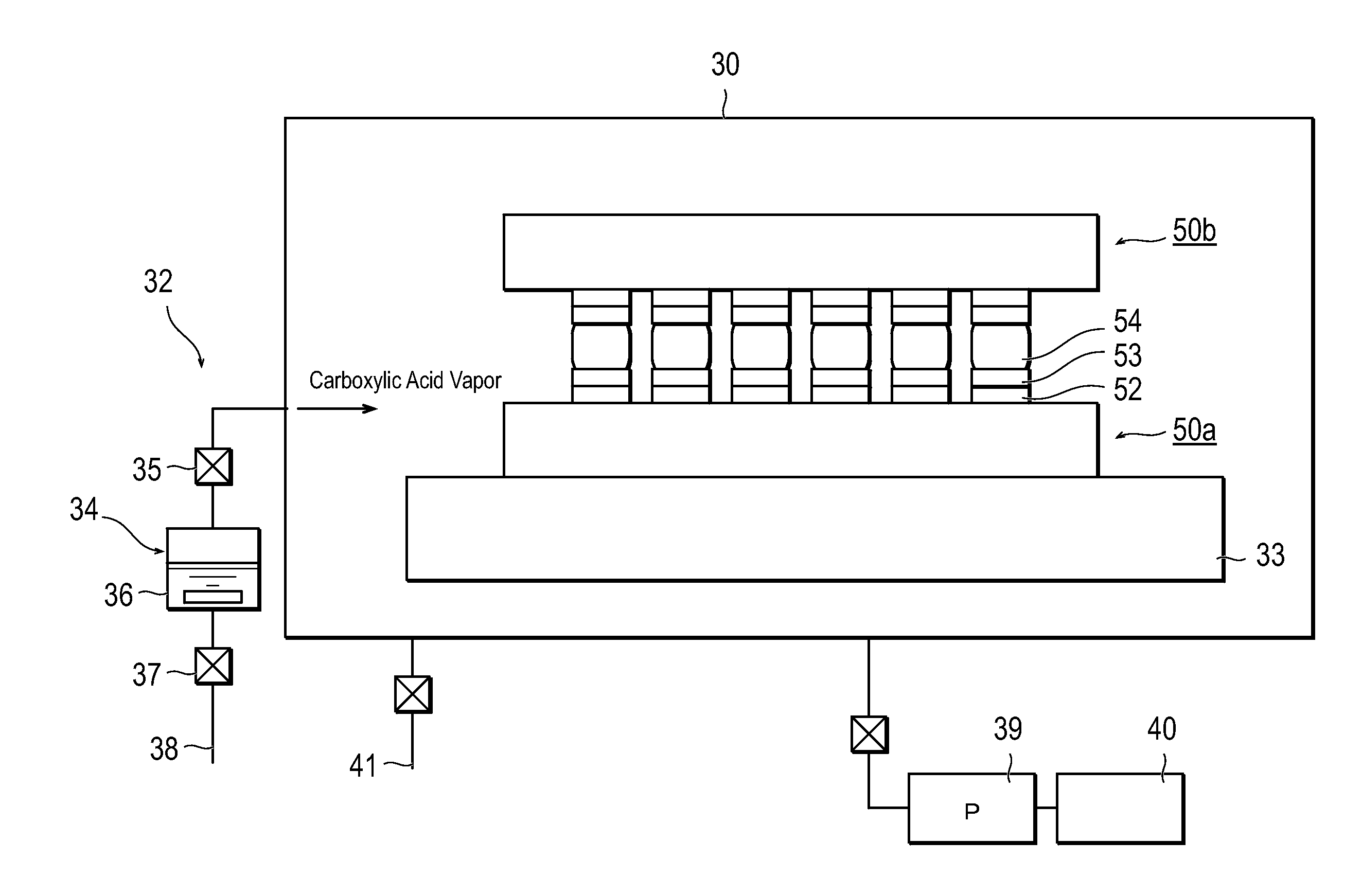
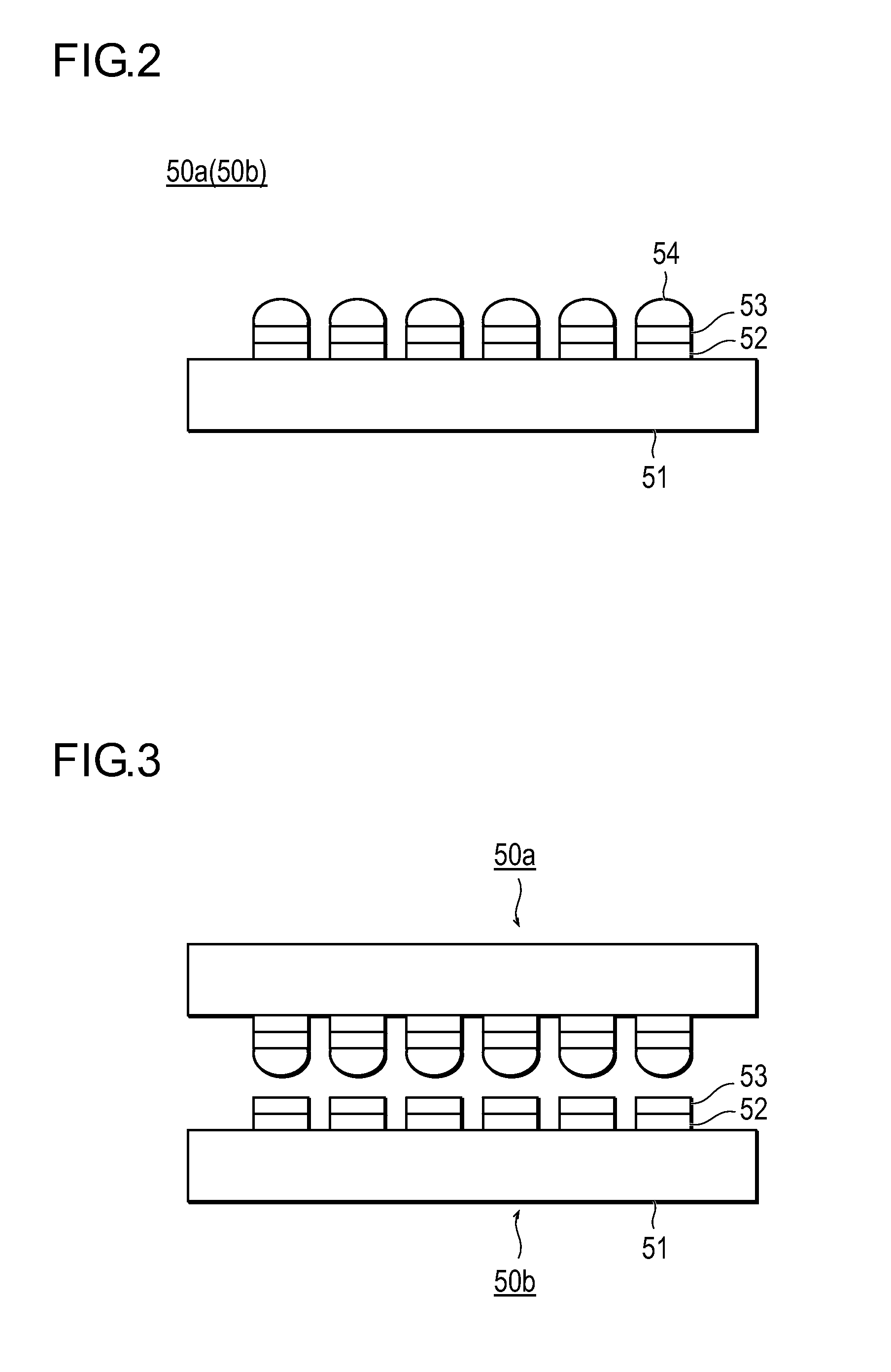
[0031]A bonding structure manufacturing technique of the first embodiment of the present invention relates to a technique for manufacturing a bonding structure by bonding multiple bonded members with solder or bonding multiple bonded members with eutectic-bonding. This bonding structure manufacturing technique can also be used for mechanical solder bonding, but preferably, the bonding structure manufacturing technique is a technique for bonding substrates with each other, bonding chips with each other, or bonding a substrate and a chip, with solder bonding, and is to electrically connect electrode structures of a pair of substrates with each other, electrically connect electrode structures of chips with each other, and electrically connect an electrode structure of a substrate and an electrode structure of a chip, with solder bonding.

[0032]It should be noted that the substrate may be an organic substrate such as a print substrate, and may be semiconductor substrate and a dielectric ...

second embodiment

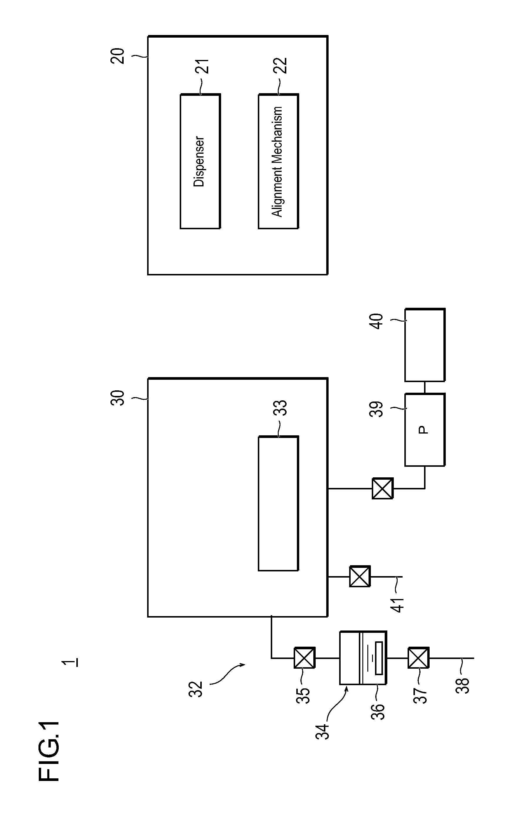
[0083]Subsequently, the second embodiment of the present invention will be explained. In the first embodiment, a case where the temporary bonding agent is applied in a planar manner onto the substrates has been explained. However, in the second embodiment, the temporary bonding agent is applied in spots manner onto multiple positions. Except this feature, the bonding structure manufacturing technique of the present embodiment is the same as the first embodiment. Accordingly, the same members as the members of the first embodiment are also denoted with the same reference numerals in the present embodiment, and detailed description thereabout is omitted.

[0084]In the present embodiment, in the temporary bonding apparatus 20 as shown in FIG. 1, the dispenser 21 dispersedly applies, in spots manner, the temporary bonding agent which is non-reducing organic agent onto the substrate surfaces formed with solder such as solder bump.

[0085]FIGS. 11(a) and 11(b) illustrate an example of a case ...

third embodiment

[0094]In the explanation about the above first and second embodiments, the temporary bonding agent which is the non-flux organic agent, i.e., the non-reducing organic agent, is applied as the temporary bonding agent 55 to the substrates, so that the substrates are temporarily bonded.

[0095]It is true that in terms of not causing migration and other contaminations even when a very small amount of temporary bonding agent 55 remains without being completely evaporated, it is desirable to use the non-reducing organic agent, which is not the flux agent, as the temporary bonding agent 55, but the present invention is not limited to this case.

[0096]More specifically, according to the present invention, multiple bonded members are temporarily bonded with the organic agent interposed therebetween, and then, before the solder is melted, the organic agent is evaporated, and therefore, even if flux agent is used as the organic agent, it is not necessary to provide a step of removing the flux by ...


PUM

PropertyMeasurementUnit
Pressureaaaaaaaaaa
Diameteraaaaaaaaaa
Diameteraaaaaaaaaa

Abstract

A soldering method capable of alleviating positional displacement between substrates even though a step of removing flux can be omitted is provided.
A temporary bonding agent 55 is applied onto multiple substrates 50a, 50b, and a heater 33 heats the substrates while the substrates are temporarily bonded with the temporary bonding agent 55 interposed therebetween, and before the solder 54 is melted or while the solder 54 is melted, the temporary bonding agent 55 is evaporated, and the substrates 50a, 50b are bonded with solder with the melted solder 54 interposed therebetween.

Description

TECHNICAL FIELD[0001]The present invention relates to a bonding structure manufacturing method, a heating and melting treatment method, and a system therefor for bonding multiple bonded members with a heat-melting material such as solder and eutectic-bonding insert metal interposed therebetween.BACKGROUND ART[0002]Techniques for manufacturing a bonding structure by bonding multiple bonded members with solder or bonding multiple bonded members with eutectic-bonding, with solder such as solder bumps or solder sheet or a eutectic-bonding insert metal interposed therebetween are widely used in semiconductor implementation steps. For example, in a semiconductor implementation step, a technique for bonding an organic substrate and a semiconductor substrate with solder with solder bumps interposed therebetween and a technique for bonding a semiconductor substrate and a semiconductor chip with solder with solder bumps interposed therebetween are employed.[0003]For example, when semiconducto...

Claims


Application Information

Patent Timeline
IPC IPC(8): B23K31/02
CPCB23K1/0016H01L2224/81193B23K2201/40B23K31/02H01L2224/81011H01L2224/75272H01L2224/7515H01L24/13H01L24/16H01L24/75H01L24/81H01L2224/13082H01L2224/13083H01L2224/81002H01L2224/81054H01L2224/81211H01L2224/81805H01L2224/81815H01L2224/81907H01L2224/8109H01L2224/75101H01L2224/83104H01L2224/81014H01L2224/81019B23K1/008H01L2224/73204H01L2224/32225H01L2224/16227H01L2224/13111H01L2224/16225H05K13/0465H01L2224/13164H01L2224/13155H01L2224/13116H01L2224/1308H01L2924/00012H01L2924/00014H01L2924/0105H01L2924/01047H01L2924/00H01L2924/01322H05K3/305H05K3/3436H05K2203/083H05K2203/085H05K2203/087B23K35/38B23K2101/40Y02P70/50B23K1/20B23K1/206B23K3/04B23K3/0607B23K3/082
Inventor ABE, HIDEYUKIMAWATARI, KAZUAKI
Owner AYUMI IND
Why Eureka
Try Eureka