
Solid-state imaging apparatus and manufacturing method of solid-state imaging apparatus

a technology of solid-state imaging and manufacturing methods, which is applied in the direction of electrical equipment, semiconductor/solid-state device manufacturing, and semiconductor devices, etc., can solve problems such as sensitivity deterioration, and achieve the effect of high reliability and easy connection between the pad and the circui

Active Publication Date: 2013-05-02
CANON KK
View PDF3 Cites 58 Cited by
  • Summary
  • Abstract
  • Description
  • Claims
  • Application Information

AI Technical Summary

Benefits of technology

The present invention provides a solid-state imaging apparatus that is reliable in its connection between the pad and circuit. Additionally, the connection between the pad and circuit can be easily formed.

Problems solved by technology

However, the finer the pixels, the smaller the light receiving area of a photoelectric conversion element for detecting light contained in each pixel, resulting in deterioration in sensitivity.

Method used


Image

  • Solid-state imaging apparatus and manufacturing method of solid-state imaging apparatus
  • Solid-state imaging apparatus and manufacturing method of solid-state imaging apparatus
  • Solid-state imaging apparatus and manufacturing method of solid-state imaging apparatus

Examples


Embodiment Construction

[0032]Various exemplary embodiments, features, and aspects of the invention will be described in detail below with reference to the drawings.

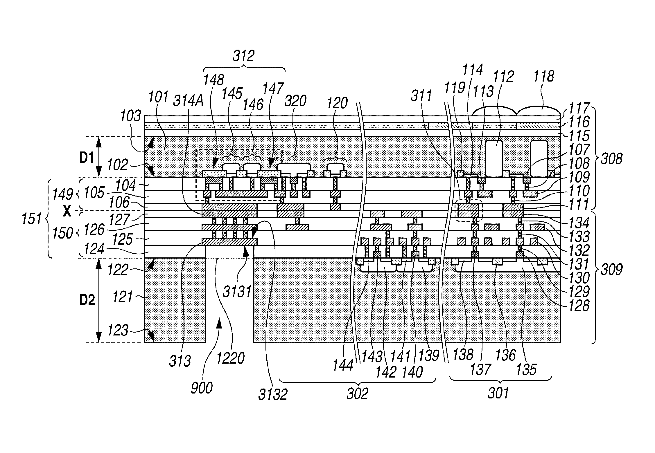
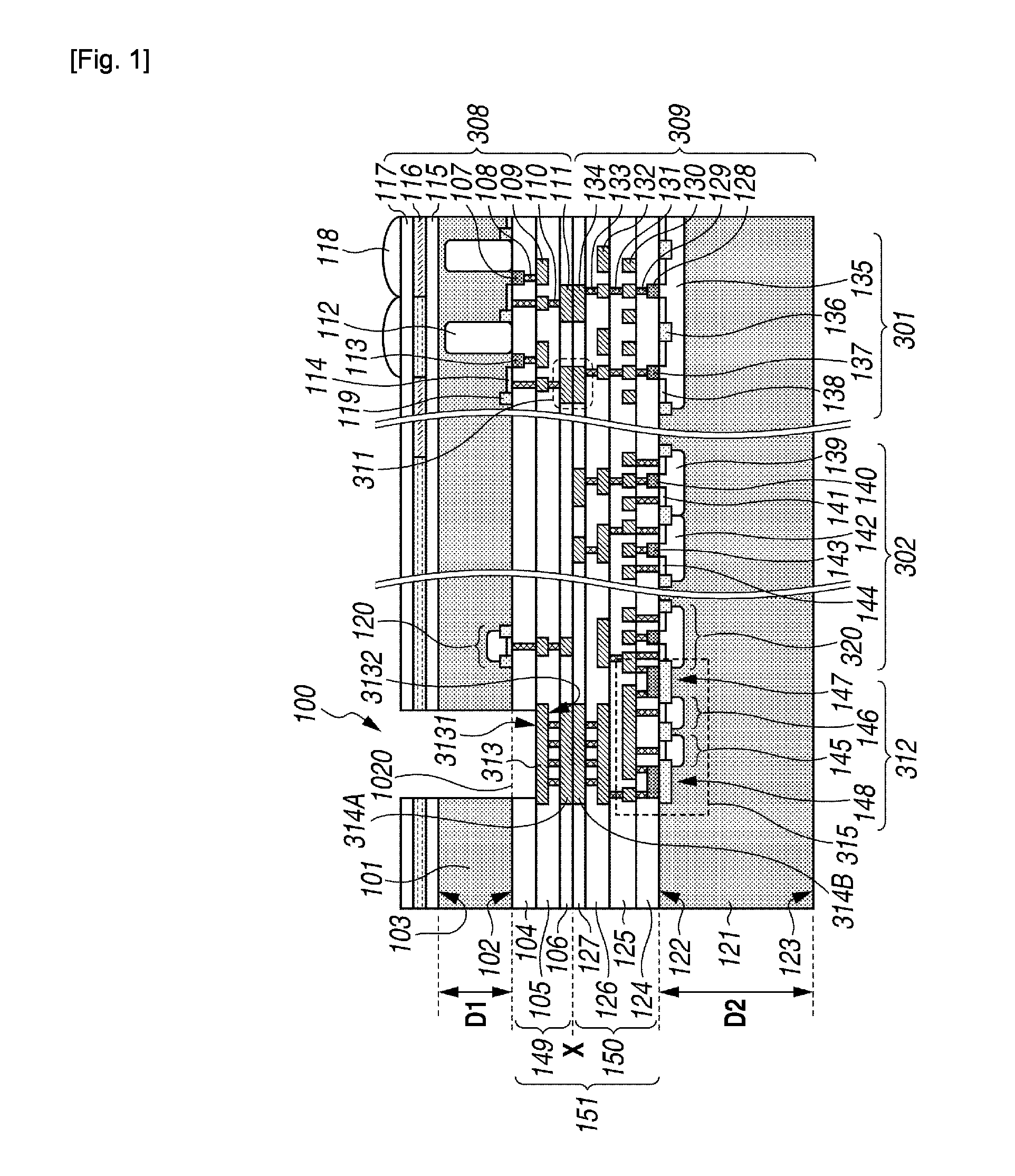
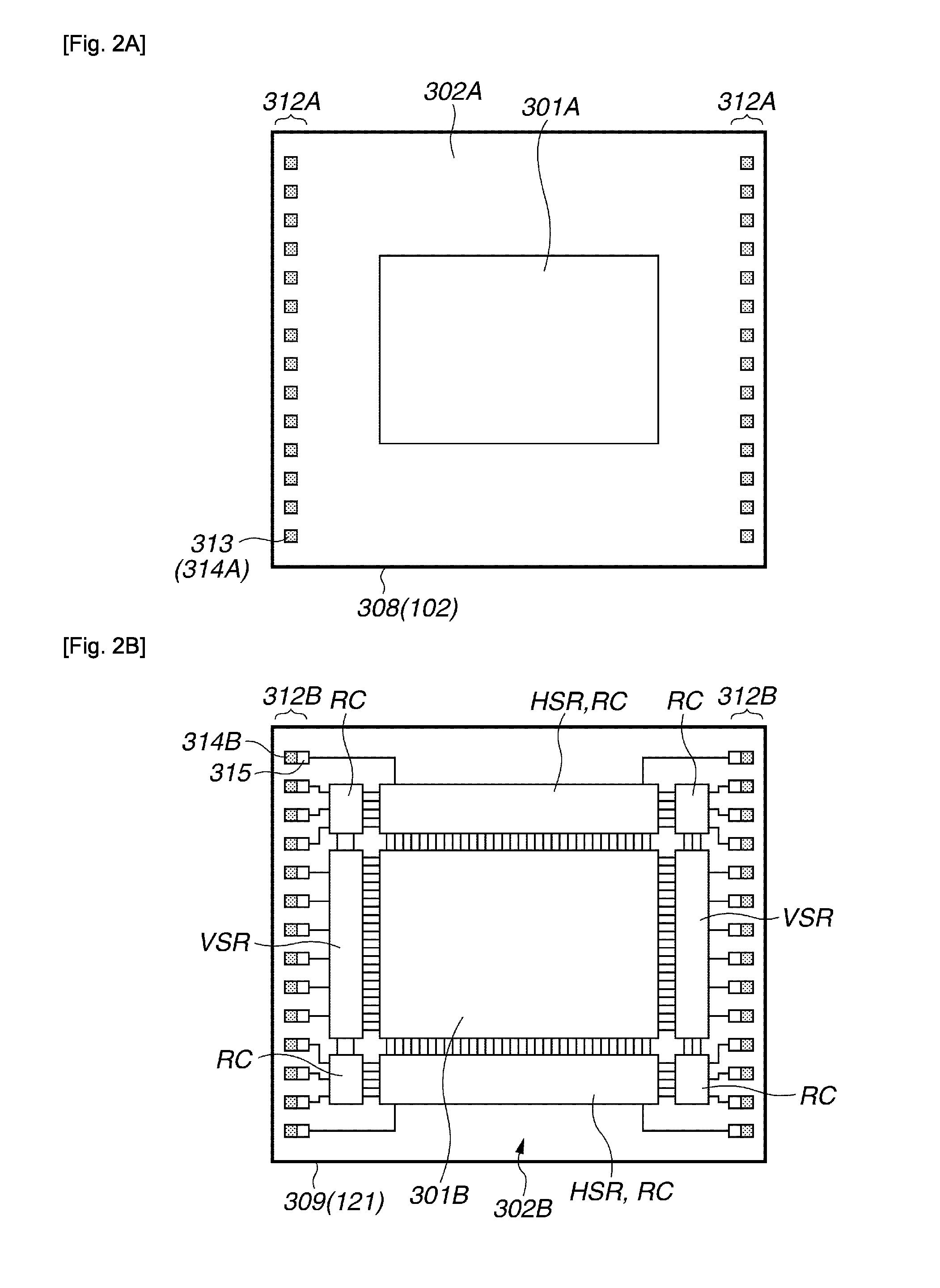
[0033]A solid-state imaging apparatus according to the present invention comprises a first semiconductor substrate including a photoelectric conversion element, and a second semiconductor substrate including at least a part of a circuit for generating a signal based on the charge of the photoelectric conversion element. The circuit is arranged in a front-side face of the second semiconductor substrate. A front-side face of the first semiconductor substrate and the front-side face of the second semiconductor substrate are arranged so as to face each other. A wiring structure is arranged between the first semiconductor substrate and the second semiconductor substrate. The solid-state imaging apparatus comprises a pad to which an external terminal is connected, and the external terminal is to be connected to a first face of the pad.

[0034]In a firs...


PUM


Abstract

The first face of the pad is situated between the front-side face of the second semiconductor substrate and a hypothetical plane including and being parallel to the front-side face, and a second face of the pad that is a face on the opposite side of the first face is situated between the first face and the front-side face of the second semiconductor substrate, and wherein the second face is connected to the wiring structure so that the pad is electrically connected to the circuit arranged in the front-side face of the second semiconductor substrate via the wiring structure.

Description

TECHNICAL FIELD[0001]The present invention relates to a solid-state imaging apparatus and, in particular, to a pad part thereof.BACKGROUND ART[0002]In a charge-coupled device (CCD) type or an amplification type solid-state imaging apparatus used in a digital still camera, a cam coder, etc, there is a demand for making pixels fine to obtain high definition images. However, the finer the pixels, the smaller the light receiving area of a photoelectric conversion element for detecting light contained in each pixel, resulting in deterioration in sensitivity.[0003]Japanese Patent Application Laid-Open No. 2006-191081 discusses a complementary metal oxide semiconductor (CMOS) type, i.e., an amplification type, solid-state imaging apparatus in which, to secure the light receiving area for the photo-electric conversion element, a first substrate on which the photoelectric conversion element and a transfer transistor are arranged and a second substrate on which another circuit is arranged are...

Claims


Application Information

Patent Timeline
Patent Type & Authority Applications(United States)
IPC IPC(8): H01L31/0224H01L31/18H04N25/00
CPCH01L27/14632H01L27/14636H01L27/1464H01L31/18H01L27/14685H01L31/0224H01L27/14645H01L27/14687H01L27/1469H01L21/76898
Inventor KOBAYASHI, MASAHIROSHIMOTSUSA, MINEO
Owner CANON KK
Learn More