Output compensation circuit and output compensation method for LCD data drive ic, and LCD

Active Publication Date: 2013-05-16
TCL CHINA STAR OPTOELECTRONICS TECH CO LTD
View PDF3 Cites 12 Cited by
  • Summary
  • Abstract
  • Description
  • Claims
  • Application Information

AI Technical Summary

Benefits of technology

The present patent is about a circuit and method to improve the output of an LCD data drive IC. The aim is to reduce the space required for the data lines, which makes it easier to create a narrow-frame LCD design. The method compensates for any inconsistency in the timing of charging signals by using delay control units to delay the output of the data drive IC from one side to the other. This ensures that each vertical column of pixel electrodes receives the same amount of charging, resulting in a uniform display. By eliminating the need for serpentine line sections, the necessary space in the glass substrate is reduced, enabling a larger number of output channels in the chip on film (COF) and reducing cost. It also improves the problem of electromagnetic interference (EMI).

Problems solved by technology

On the other hand, if the impedances of the data lines are designed to be inconsistent with each other, then the charging time of the pixels in the same row would vary from each other to cause non-uniformity of the image displayed in the region controlled by the corresponding data lines.
Therefore, the existing wiring scheme in the form of serpentine line sections fails to satisfy the requirements of a small wiring space and uniform displaying of an image.
Furthermore, the existing data drive IC 3 outputs signals from the output channels simultaneously, so a large current has to be provided to the glass substrate when all the output channels are opened, which will lead to the problem of electromagnetic interference (EMI).

Method used


Image

  • Output compensation circuit and output compensation method for LCD data drive ic, and LCD
  • Output compensation circuit and output compensation method for LCD data drive ic, and LCD
  • Output compensation circuit and output compensation method for LCD data drive ic, and LCD

Examples


Embodiment Construction

[0049]It shall be understood that, the embodiments described herein are only intended to illustrate but not to limit the present disclosure.

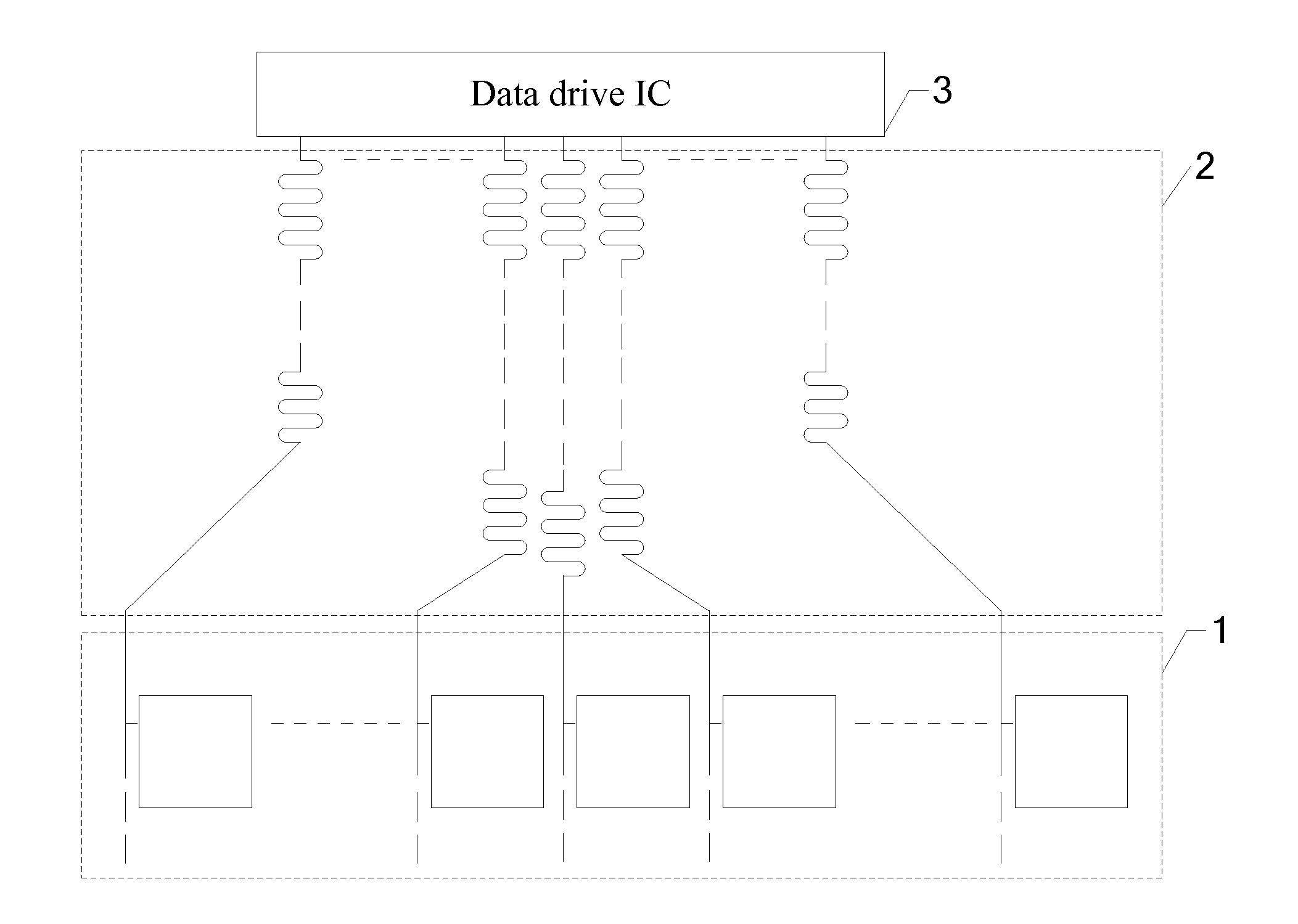
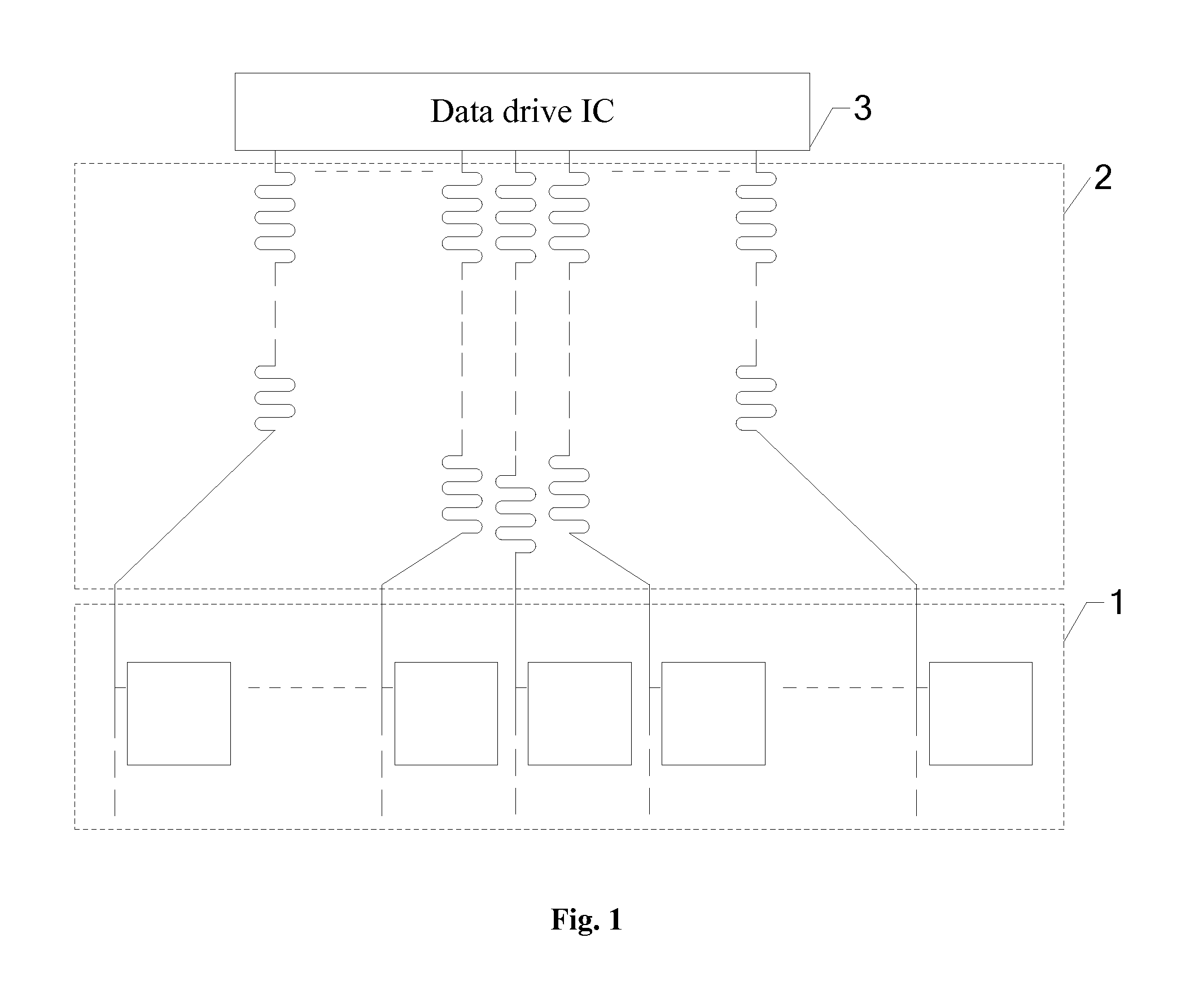
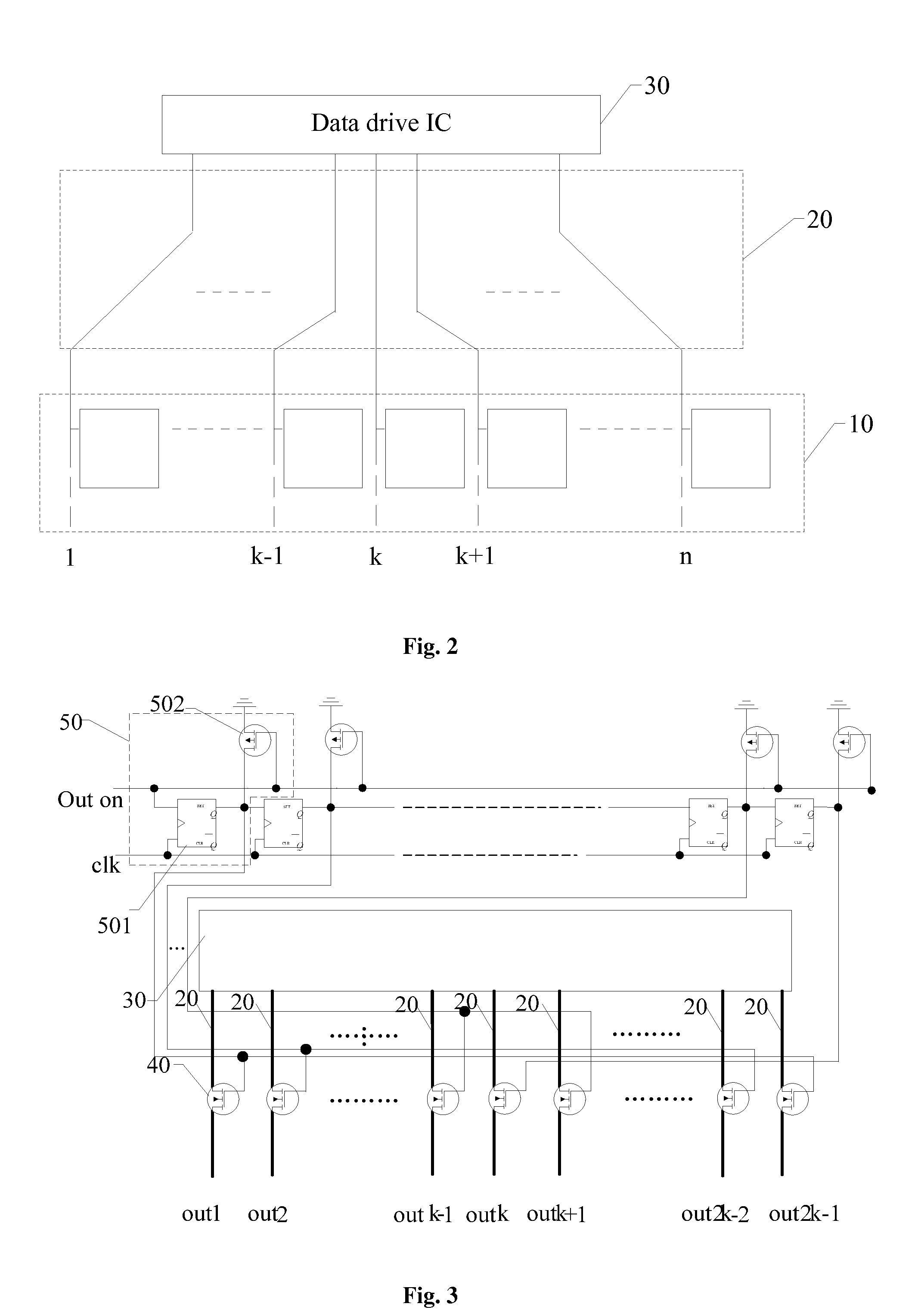
[0050]The primary solution of the present disclosure is as follows: output control switches are disposed in output channels of a data drive IC, and are turned on stage by stage by delay control units according to impedance values of data lines so that the charging time is the same for pixel electrodes in each row on a glass substrate, which ensures uniformity of the image displayed; and because the need of serpentine line sections is eliminated for the data lines, the wiring space is reduced, which is favorable for the narrow-frame design of the LCD.

[0051]Referring to FIG. 2 and FIG. 3 together, FIG. 2 is a schematic structural view illustrating data lines outputted from a data drive IC that charge pixel electrodes without the need of wiring according to the present disclosure; and FIG. 3 is a schematic structural view illustrating an output com...


PUM


Abstract

An output compensation circuit and an output compensation method for an LCD data drive IC as well as an LCD comprising the same are disclosed. The output compensation circuit comprises a data drive IC, a plurality of first switch units and a plurality of delay control units. A plurality of output channels of the data drive IC each are connected with a corresponding row of pixel electrodes on a glass substrate via a data line respectively to output a charging signal. Each of the first switch units control the corresponding output channel according to a delay control signal generated by the corresponding delay control unit. Each of the delay control units is configured to generate the delay control signal-used to control the first switch unit to be turned on after a predetermined delay so that the charging time is the same for all the pixel electrodes.

Description

BACKGROUND[0001]1. Technical Field[0002]The present disclosure relates to the technical field of liquid crystal display, and more particularly, to an output compensation circuit and an output compensation method for a liquid crystal display (LCD) data drive integrated circuit (IC) that facilitate a narrow-frame design of an LCD, and the LCD comprising the same.[0003]2. Description of Related Art[0004]FIG. 1 shows data lines 2 in an LCD panel. In order for signals of the data lines 2 outputted by a data drive integrated circuit (IC) 3 to reach pixels of each row at the same time, impedances of the data lines 2 must be made substantially the same. In order to make the impedances of the routing lines connected to the pixels substantially the same, a serpentine line section is usually used in the prior art. Each of the data lines 2 is connected to a pixel region 1 via a serpentine line section, and the impedances of the data lines 2 are made substantially the same through selection of t...

Claims


Application Information

Patent Timeline
IPC IPC(8): G09G3/36G09G5/00
CPCG09G5/00G06F3/041G09G3/3688G09G2330/06G09G2320/0223G09G2320/0233G09G2310/08
Inventor LIAO, LIANG-CHANLIN, PO-SHENGUO, DONGSHENG
Owner TCL CHINA STAR OPTOELECTRONICS TECH CO LTD
Why Eureka
Try Eureka