Semiconductor process

a technology of semiconductors and process steps, applied in the direction of semiconductor devices, electrical devices, transistors, etc., can solve the problems of collateral damage of the target material, the pre-amorphization implant method still has some drawbacks, and the element is more susceptible to unintended effects, so as to improve the speed and reliability of the device

Active Publication Date: 2013-05-30
UNITED MICROELECTRONICS CORP
View PDF4 Cites 18 Cited by
  • Summary
  • Abstract
  • Description
  • Claims
  • Application Information

AI Technical Summary

Benefits of technology

[0007]The present invention proposes multiple possible novel semiconductor processes. The novel semiconductor processes of the present invention include at least one implanting step carried out in a cryogenic procedure. The novel semiconductor processes of the present invention prevent the epitaxial strained material from

Problems solved by technology

Although the implantation of the dopant comes with the benefits of adjustment of the electrical properties of the semiconductor elements, the damages on the materials coming with the implantation of the dopant usually make the elements more susceptible to unintended effects.
However, the pre-amorphization implant method

Method used


Image

  • Semiconductor process
  • Semiconductor process
  • Semiconductor process

Examples


Embodiment Construction

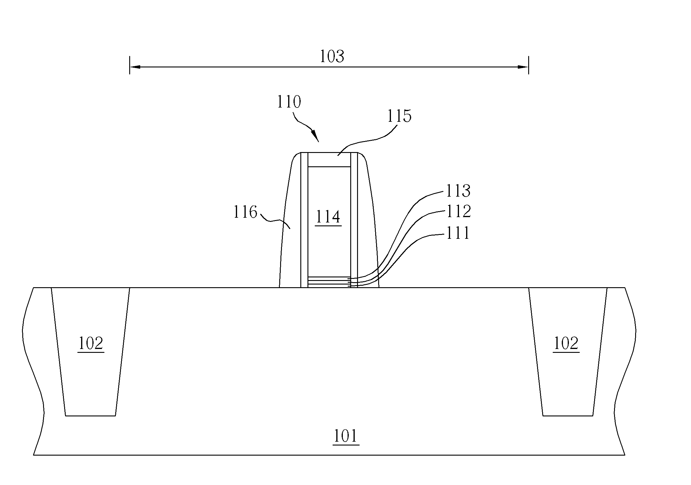
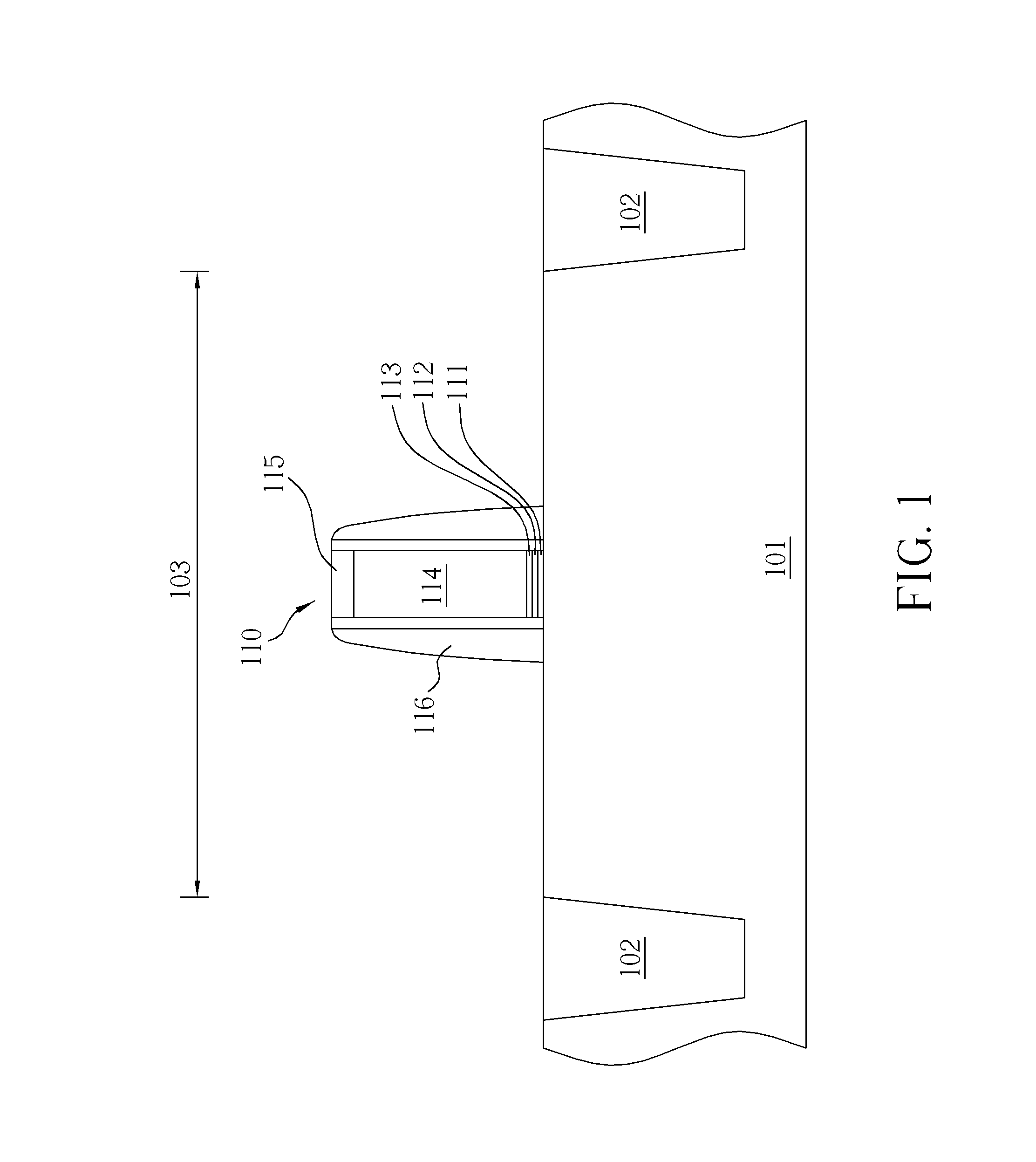
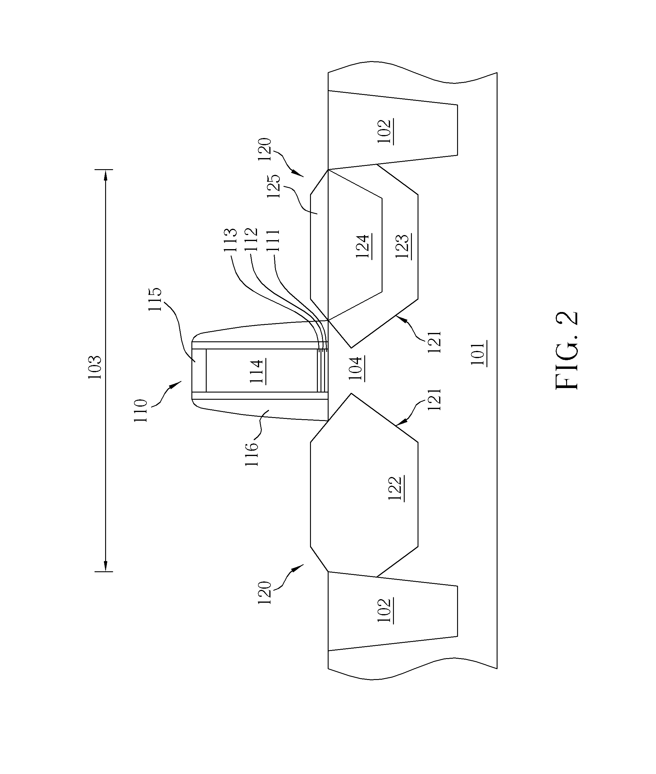
[0026]The present invention proposes multiple novel semiconductor processes which are carried out in a cryogenic procedure. The novel semiconductor processes of the present invention include at least one implanting step, such as a pre-amorphization implanting step or a source / drain implanting procedure, in a cryogenic condition. The novel semiconductor processes of the present invention prevent the epitaxial material from forming dislocations after the pre-amorphization implanting step, and prevent problems such as dislocation flaws, low junction leakage or relaxation of the stress so as to further provide a semiconductor element of better reliability.

[0027]FIGS. 1 to 8 illustrate some semiconductor processes carried out in a cryogenic procedure of the present invention, such as semiconductor processes for fabricating MOS by epitaxial or stress memorization techniques (SMT). First, as shown in FIG. 1, a substrate 101 is provided. The substrate 101 may be a semiconductive material, s...


PUM


Abstract

First, a substrate with a recess is provided in a semiconductor process. Second, an embedded SiGe layer is formed in the substrate. The embedded SiGe layer includes an epitaxial SiGe material which fills up the recess. Then, a pre-amorphization implant (PAI) procedure is carried out on the embedded SiGe layer to form an amorphous region. Next, a source/drain implanting procedure is carried out on the embedded SiGe layer to form a source doping region and a drain doping region. Later, a source/drain annealing procedure is carried out to form a source and a drain in the substrate. At least one of the pre-amorphization implant procedure and the source/drain implanting procedure is carried out in a cryogenic procedure below −30° C.

Description

BACKGROUND OF THE INVENTION[0001]1. Field of the Invention[0002]The present invention generally relates to a semiconductor process including at least one of an implanting procedure. In particular, the present invention is directed to a semiconductor implanting process carried out in a cryogenic procedure below −30° C. to prevent the epitaxial material from forming dislocations.[0003]2. Description of the Prior Art[0004]Implanting procedures are usually employed in the conventional semiconductor processes to implant the needed dopant. Although the implantation of the dopant comes with the benefits of adjustment of the electrical properties of the semiconductor elements, the damages on the materials coming with the implantation of the dopant usually make the elements more susceptible to unintended effects. In order to solve the dilemma, this technical field thus develops a precise damage engineering. This enhancing amorphization technique enhances the amorphization by implantation to ...

Claims


Application Information

Patent Timeline
IPC IPC(8): H01L21/20
CPCH01L29/517H01L29/6656H01L29/6659H01L29/7848H01L29/7834H01L29/7847H01L29/66636
Inventor YANG, CHAN-LONLI, CHING-ILIN, GER-PINLAI, I-MINGHUANG, YUN-SANLIAO, CHIN-ICHIEN, CHIN-CHENG
Owner UNITED MICROELECTRONICS CORP
Why Eureka
Try Eureka