

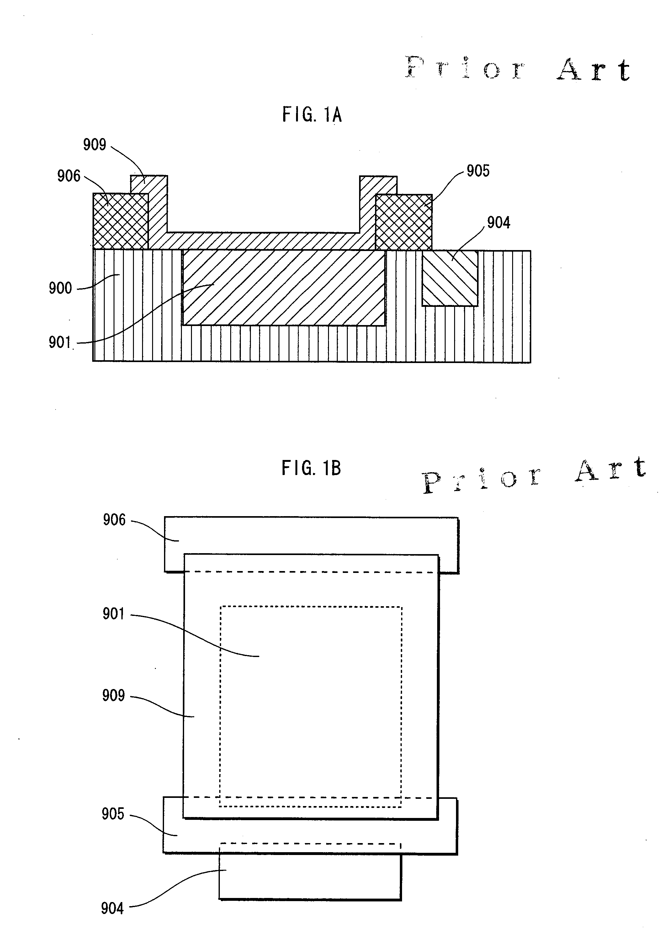
Solid-state imaging device having transmission gates which pass over part of photo diodes when seen from the thickness direction of the semiconductor substrate
a technology of transmission gate and semiconductor substrate, which is applied in the direction of semiconductor devices, radio frequency controlled devices, electrical devices, etc., can solve the problems of lowering the sensitivity characteristic, reducing the resistance of the transmission gate, and blocking or absorbing part of the incident ligh
- Summary
- Abstract
- Description
- Claims
- Application Information
AI Technical Summary
Benefits of technology
Problems solved by technology
Method used
Image

Examples
first embodiment
[0054]1. General Structure of Solid-State Imaging Device 1
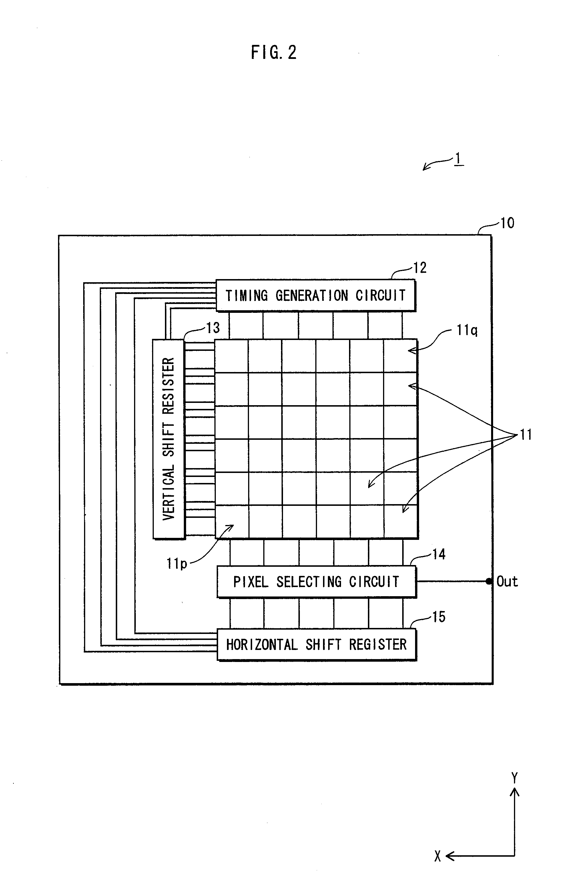
[0055]The following describes a general structure of a solid-state imaging device 1 of the first embodiment, with reference to FIG. 2, which is a schematic block view that shows a general structure of the solid-state imaging device 1 of the present embodiment. The solid-state imaging device 1 has a MOS-type structure, and is used as an imaging device in a digital still camera or a movie digital camera.
[0056]As shown in FIG. 2, the solid-state imaging device 1 of the present invention has a semiconductor substrate 10 as a base, and along one main surface thereof, (i) a plurality of image pixels 11 that are arranged in a matrix state and (ii) circuit units that are connected to each image pixel 11, are formed.
[0057]The circuit units of the solid-state imaging device 1 include a timing generation circuit 12, a vertical shift register 13, a pixel selecting circuit 14, and a horizontal shift register 15. The vertical shift registe...
second embodiment
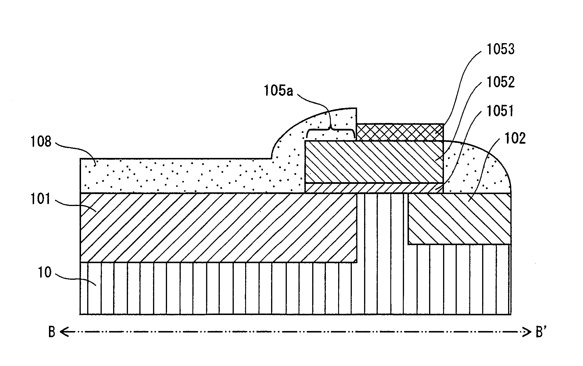
[0103]The following describes the solid-state imaging device of the second embodiment, with reference to FIG. 9A and FIG. 9B. It should be noted that, in the solid-state imaging device of the present embodiment, the descriptions of the structures excluding the arrangement of the photodiode 101 and the transmission gate 205 are omitted since the descriptions are the same as the solid-state imaging device of the above-described first embodiment. In the structure of the solid-state imaging device of the present embodiment, FIG. 9A is the schematic planar view that shows the arrangement of the photodiode 101 and the transmission gate 205, and FIG. 9B is a schematic sectional view that shows the structure of the periphery of the photodiode 101 (a cross-sectional surface of C-C′ of FIG. 9A).
[0104]As shown in FIG. 9A, in the solid-state imaging device of the present embodiment, as is the case with the image pixel 11 of the solid-state imaging device of the above-described first embodiment,...
third embodiment
[0116]The following describes a solid-state imaging device of the third embodiment, with reference to FIG. 11A and FIG. 11B. FIG. 11A is a schematic view that shows the photodiode 101 and the transmission gate 305 in the image pixel 31, which are the most distinctive characteristics in the structure of the solid-state imaging device of the present embodiment. FIG. 11B is a schematic view that shows the photodiode 101 and the transmission gate 605 in the image pixel 61 as a variation.
[0117]As shown in FIG. 11A, as is the case with the solid-state imaging devices of the above-described first and second embodiments, the image pixel 31 of the solid-state imaging device of the present embodiment has a structure in which part of the transmission gate 305 passes over the photodiode 101, and the part thereof passes over one side of the periphery of the rectangular shaped photodiode 101 in the oblique direction. The difference between (i) the image pixel 31 of the present embodiment and (ii)...
PUM
 Abstract
Description
Claims
Application Information