Solid-state imaging device and production method of the same

a technology of solid-state imaging and production method, which is applied in the direction of color television, television system, radio control device, etc., can solve the problems of increased manufacturing cost, increased manufacturing cost, increased manufacturing cost, etc., and achieves the effect of reducing leakage generating factors, reducing damage, and improving transistor operating characteristics

Inactive Publication Date: 2005-07-07
SHARP KK
View PDF7 Cites 8 Cited by
  • Summary
  • Abstract
  • Description
  • Claims
  • Application Information

AI Technical Summary

Benefits of technology

[0035] The gate insulating film and the light receiving region covering film function as a film for reducing damage when a side wall is formed, thereby making it possible to reduce leakage generating factors. Further, forming a silicide layer on a source region and a drain region of the transistor and a surface of the gate electrode, thereby making it possible to improve operating characteristics of the transistor. When the silicide layer is formed, the insulating film on the light receiving region functions as a film for preventing the formation of a silicide layer, thereby making it possible to prevent a reduction in sensitivity characteristics of the light receiving region.
[0036] Further, the gate insulating film and the light receiving region covering film may be each a multilayer film comprising two or more insulating films having different refractive indexes, thereby making it possible to function as an antireflection film. Therefore, a surface reflectance of the light receiving region can be reduced, thereby making it possible to improve the sensitivity characteristics.
[0037] Thus, according to the present invention, the surface of a diffusion layer serving as the source region and the drain region of the transistor and the surface of the gate electrode are made of silicide, thereby making it possible to reduce the resistance, and therefore, improve the operating speed of the transistor and reduce the operating voltage thereof. Further, the gate insulating film of the transistor and the insulating film (light receiving region covering film) covering the surface of the light receiving region (photodiode) can be formed simultaneously, whereby it is no longer necessary to provide a silicide formation preventing film. Furthermore, the gate insulating film and the light receiving region covering film can also function as a film for reducing damage when a side wall is formed. Therefore, it is possible to avoid leakage generating factors in addition to a reduction in manufacturing cost.
[0038] Furthermore, the gate insulating film and the light receiving region covering film may be each a multilayer film comprising two or more insulating films having different refractive indexes, thereby making it possible to reduce manufacturing cost and reduce the surface reflectance of the light receiving region to improve the sensitivity characteristics of the photodiode.
[0039] Thus, the invention described herein makes possible the advantages of providing a solid-state imaging device having improved operating characteristics of a MOS transistor and improved sensitivity characteristics of a photodiode and capable of being produced with low cost; and a production method thereof.

Problems solved by technology

To avoid this, the step of forming a film for preventing the formation of silicide in the photodiode portion is required, resulting in an increase in manufacturing cost.
To avoid this, the step of forming the multilayer antireflection film 55 in the photodiode portion is required, resulting in an increase in manufacturing cost.
Further, in the conventional MOS image sensor 100 having the silicide layer 60, the step of forming the gate oxide film 57 (gate insulating film) of the MOS transistor 53 and the step of forming the silicide prevention film are requited in addition to the step of forming the multilayer antireflection film 55 for covering the surface of the photodiode 52, resulting in an increase in manufacturing cost.

Method used


Image

  • Solid-state imaging device and production method of the same
  • Solid-state imaging device and production method of the same
  • Solid-state imaging device and production method of the same

Examples


Embodiment Construction

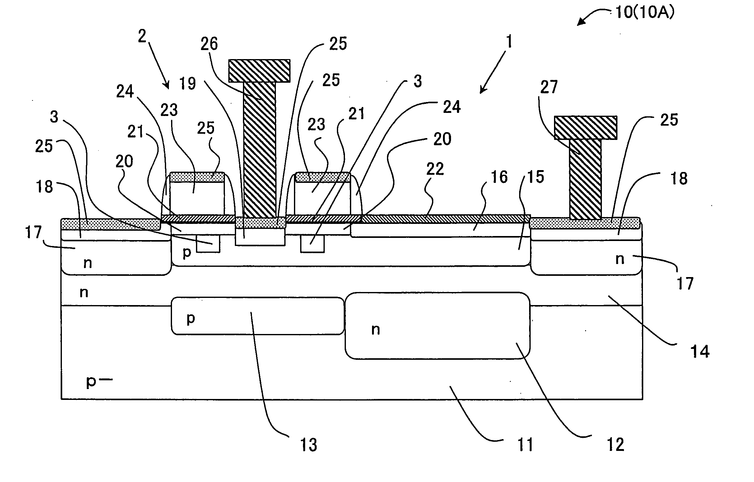
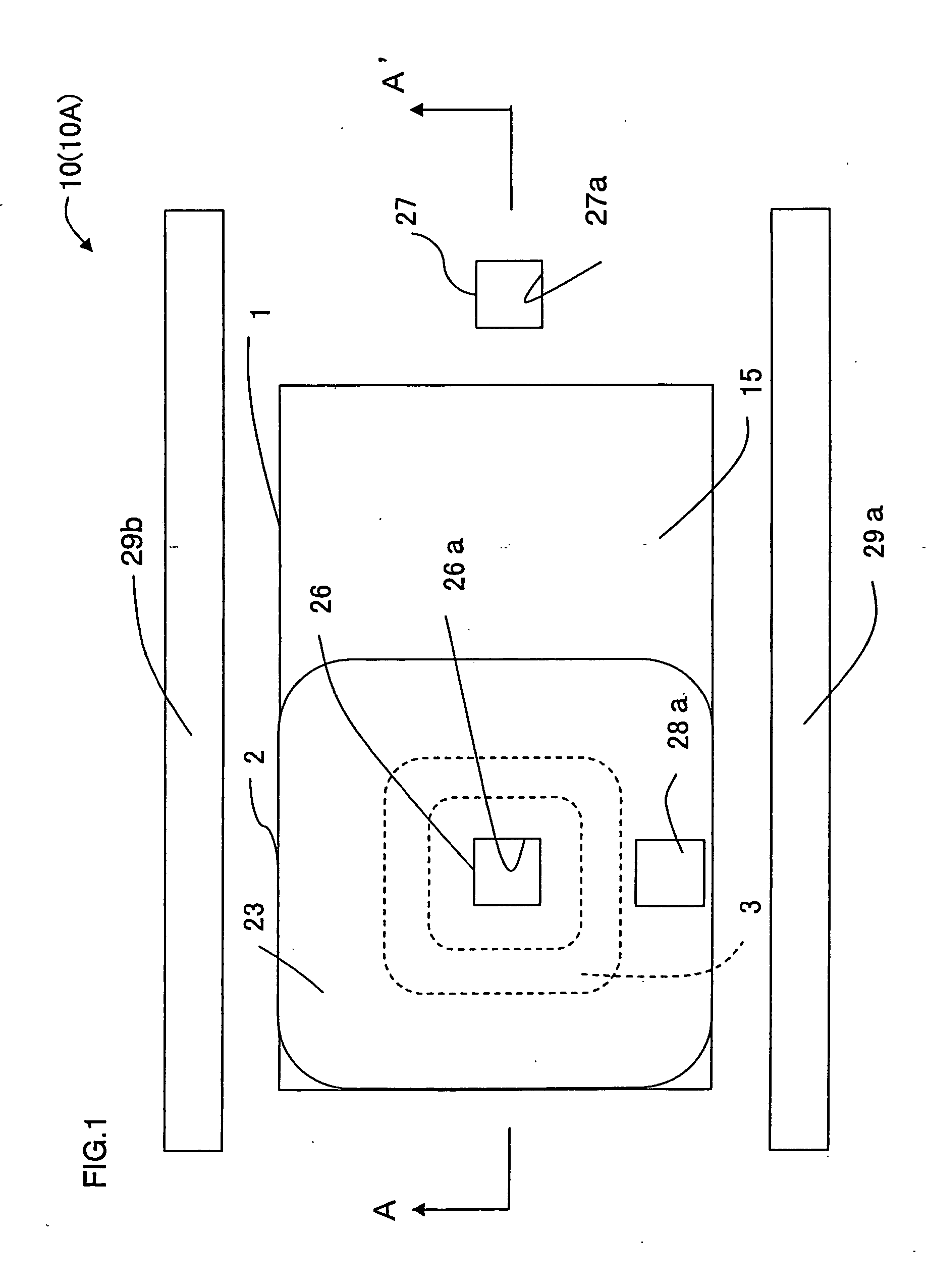
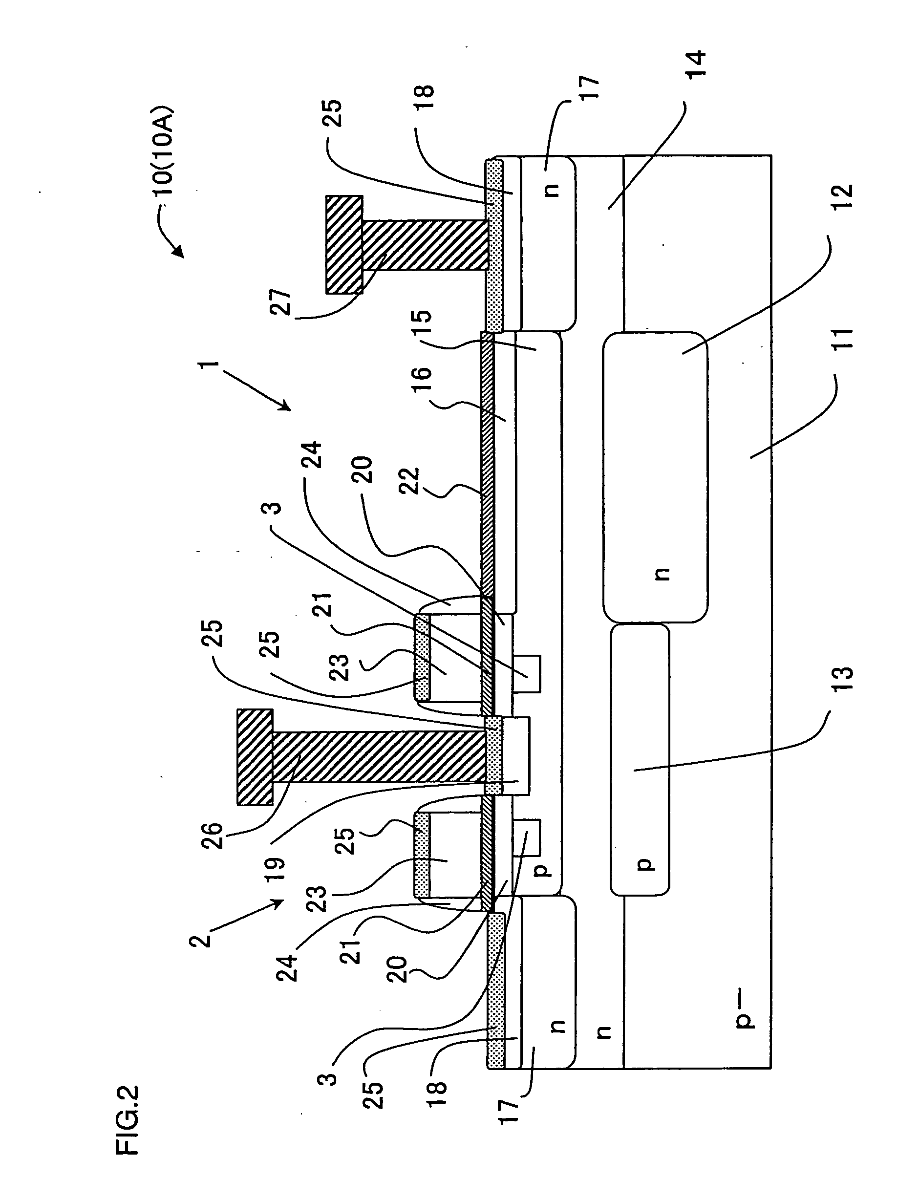
[0047] Hereinafter, the present invention will be described by way of illustrative examples with reference to the accompanying drawings. Particularly, a threshold voltage modulation MOS image sensor is described as a solid-state imaging device of the present invention.

[0048]FIG. 1 is a plane view showing an exemplary unit pixel portion in a threshold voltage modulation MOS image sensor according to an embodiment of the present invention. FIG. 2 is a cross-sectional view of the unit pixel portion, taken along line A-A′ in FIG. 1. Note that the MOS image sensor (solid-state imaging device) has a plurality of unit pixel portions arranged in rows and columns (i.e., in a matrix (in a two-dimensional manner)) though not shown in FIGS. 1 and 2.

[0049] In FIGS. 1 and 2, the unit pixel portion 10A of the MOS image sensor 10 of the embodiment of the present invention has a light receiving diode 1 (photodiode) for photoelectric conversion, a MOS transistor 2 for detecting a light signal, whic...


PUM


Abstract

A solid-state imaging device is provided, which comprises unit pixel portions. Each unit pixel portion comprises a first conductivity type substrate, a second conductivity type semiconductor layer, a first conductivity type well region, a light receiving region for generating electric charges when irradiated with light, an electric charge accumulation region for accumulating the electric charges from the light receiving region, and a transistor capable of reading out a signal corresponding to an amount of the electric charges accumulated in the electric charge accumulation region. A surface of the light receiving region is covered with an insulating film made of the same material as that of a gate insulating film of the transistor.

Description

[0001] This nonprovisional application claims priority below 35 U.S.C. §119(a) on Patent Application No. 2003-408343 filed in Japan on Dec. 5, 2003, the entire contents of which are hereby incorporated by reference. BACKGROUND OF THE INVENTION [0002] 1. Field of the Invention [0003] The present invention relates to a solid-state imaging device, a threshold voltage modulation MOS image sensor, or the like, which is used in, for example, a camcorder, a digital camera, a cellular telephone with camera and the like; and a production method of the same. [0004] 2. Description of the Related Art [0005] Conventionally, a CCD image sensor, a MOS image sensor and the like are known as solid-state imaging devices which convert image light to an electrical signal (image signal). The MOS image sensor has a light receiving region (photodiode), which generates electric charges when irradiated with light, and a transistor (MOS transistor), which reads out the electric charge generated in the light ...

Claims


Application Information

Patent Timeline
Patent Type & Authority Applications(United States)
IPC IPC(8): H01L31/062H01L27/146H01L31/10H04N5/335H04N5/369H04N5/374
CPCH01L27/14609H01L27/14689H01L27/14643H01L27/1462H01L27/146H01L31/10H04N25/76
Inventor IWATA, HIROSHI
Owner SHARP KK
Why Eureka
Try Eureka