Waveguide raman scattering cavity based on twice-coupling prism
A Raman scattering and prism technology, applied in the field of waveguide Raman scattering cavity, can solve the problems of insufficient Raman spectral sensitivity and narrow application range, and achieve the effects of Raman scattering enhancement, interference elimination, and scattering cross section enhancement
- Summary
- Abstract
- Description
- Claims
- Application Information
AI Technical Summary
Problems solved by technology
Method used
Image
Examples
Embodiment 1
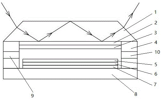
[0019] Example 1: please combine figure 1 As shown, the structure of the waveguide Raman scattering cavity with twice coupled prisms involved in this embodiment is a glass prism 1, an upper silver film 2, an upper silicon dioxide protective film 3, a glass gasket 4, and a lower layer from top to bottom. A silicon dioxide protective film 5 , a lower silver film 6 , a glass substrate 7 , and a glass substrate 8 . The upper silver film 2 and the upper silicon dioxide protective film 3 are deposited on the bottom surface of the glass prism 1 successively, and the lower silver film 6 and the lower silicon dioxide protective film 5 are successively deposited on the surface of the glass substrate 7, and then the glass prism 1, the glass The gasket 4, the glass substrate 7 and the glass substrate 8 are combined into one body by photoresist technology. The materials of glass substrate 7 and glass substrate 8 are both optical glass, and the thickness of glass substrate 7 is smaller tha...
Embodiment 2
[0023] Example 2: please combine Figure 4 The structure of the waveguide Raman scattering cavity with twice coupled prisms shown can also be a glass prism 101, an upper layer of silver film 102, an upper layer of silicon dioxide protective film 103, a glass gasket 104, and a lower layer of silicon dioxide protective film from top to bottom. film 105, lower silver film 106, glass substrate 107. The upper silver film 102 and the upper silicon dioxide protective film 103 are deposited on the bottom surface of the glass prism 101 successively, and the lower silver film 106 and the lower silicon dioxide protective film 105 are deposited on the surface of the glass substrate 107 successively, and then the glass prism 101, the glass gasket 104 and the glass substrate 107 are combined into one body by photoresist technology. A cavity for storing liquid samples to be tested is formed between the glass prism 101 and the glass substrate 107 . Two through holes are opened on the glass ...
PUM
| Property | Measurement | Unit |
|---|---|---|
| angle | aaaaa | aaaaa |
| thickness | aaaaa | aaaaa |
| thickness | aaaaa | aaaaa |
Abstract
Description
Claims
Application Information


