[0008]Optical emission measurements are well suited for in-situ
metrology and diagnostics during
pulsed laser processing of materials in real time. Optical emission can provide excellent specificity to
chemical composition of the processed material and can be measured very fast.
Optical measurements do not require vacuum and can be implemented in a contact-less configuration from a stand-off distance. Accordingly, it is desirable to have a method of
optical diagnostics that can be applied in-situ during
laser ablation and laser
processing in real time. This method can be
fully automated and enables high efficiency and
throughput in manufacturing at the best attainable precision and minimization of damage to the products.
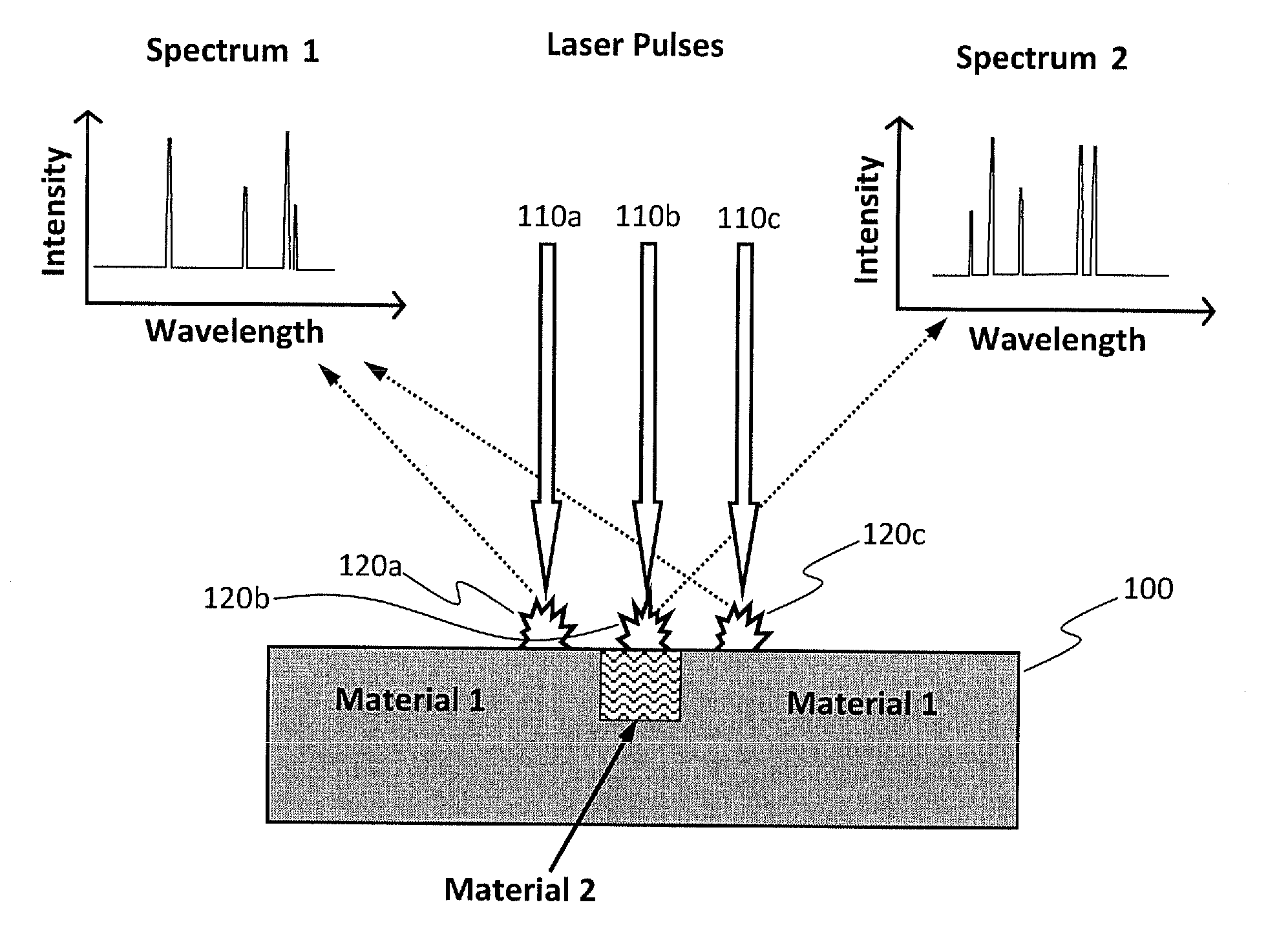
[0009]By combining a scanable processing laser with an optical emission detection
system and a
control system, used as an optical diagnostics
system, the laser can form blind holes or can be scanned across the multilayered electronic structures to remove the desired
layers without causing damage to the underlying layers. An optical detection and analysis
system can distinguish in real time between the material to be removed from the underlying materials. As soon as the material from the underlying layer is detected in the
laser ablation plume by the optical diagnostics system, either the laser is stopped or the laser's power is reduced to prevent damage of the underlying layer.
[0012]In one illustrative embodiment, optical emission is collected with at least one lens and coupled via a fiberoptic cable to a measuring device, preferably an optical
spectrograph fitted with a CCD or ICCD camera, which digitizes the
spectral data for further
computational analysis in real time. In this fashion, the present invention enables the practitioners to realize the disclosed method of optical diagnostics from a stand-off distance without direct contact with the ablated material. Therefore, no physical disturbance or interference with the material processing is required to implement the provided optical diagnostic method. The stand-off distance will preferably be small in order to facilitate efficient collection of the optical emission. However, the stand-off distance can be increased to several meters or tens of meters, if so desired.
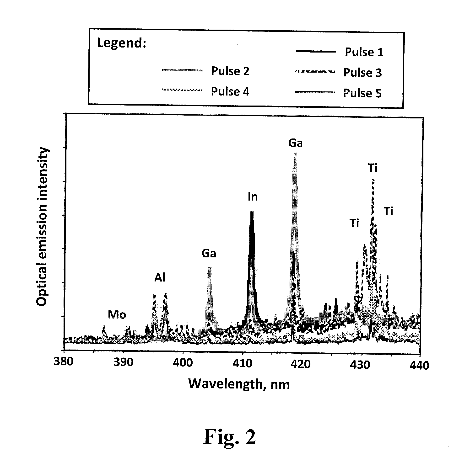
[0013]In another illustrative embodiment, a CCD or ICCD camera is synchronized with the individual laser
ablation pulses in such a way that optical emission is measured with an appropriate
delay after a laser pulse and only during a gated period of time. The
delay and the gate width are optimized to enhance useful spectral features, while concurrently decreasing continuum background in laser-generated optical spectra. When a
pulsed laser with a high repetition rate is used for material ablation, the fast on-
chip accumulation of
spectral data in the pixels of the CCD or ICCD camera integrated over multiple laser pulses can be preferred in order to increase the
signal-to-
noise ratio. Alternatively,
spectral data from each individual pulse can be measured to detect a change of
chemical composition of the material in a technique often referred to as “end-point detection.”
[0015]In accordance with another aspect of the present invention, computational
statistical analysis of digital spectral data can be further implemented to identify and characterize the ablated material on the basis of the measured spectra. Aforesaid
statistical analysis is often referred to as “chemometric analysis” or “
chemometrics.” In the present invention, the chemometric algorithms will compare a real-time measured spectrum to the spectra stored in a
reference database in memory of a system computer. This method allows practitioners to identify, discriminate and characterize the ablated materials in a real-time automated mode of operation. This method can be used to discriminate between materials of similar
elemental composition, but of different molecular structure. Some physical properties of the materials, such as reflectance or density, and certain crystallographic structures can also be discriminated in many cases. Accordingly, material compositional and
structural consistency or deviations from thereof during the process can be monitored in real time.
[0020]In some embodiments, the measuring comprises measuring spectral intensities using optical
spectroscopy in a broad sense that involves
electromagnetic radiation, which can be
microwave, terahertz,
infrared, visible,
ultraviolet, or x-
ray radiation. In some embodiments, the measuring further comprises measuring using a spectroscopic apparatus which collects and detects
electromagnetic radiation such as light from a stand-off distance without direct contact with the ablated material. In some embodiments, the measuring further comprises measuring using accumulation of the spectral data with a coupled charge device (CCD) or intensified CCD (ICCD) camera over multiple laser pulses. In some embodiments, the measuring further comprises measuring using fast-gated direct accumulation of the spectral data on the
chip of an ICCD camera over multiple laser pulses, wherein gated on-
chip accumulation facilitates enhancing at least one useful spectral feature while concurrently decreasing continuum background in laser-generated optical spectra.

