Solid-state infrared imager

a solid-state infrared and imager technology, applied in the direction of instruments, radiation controlled devices, optical radiation measurement, etc., can solve the problems of limiting the signal bandwidth, the cooling system is required for low-temperature operation, and the problem of solid-state infrared imagers have some problems, etc., to achieve high sensitivity, low noise level, and wide dynamic range

Inactive Publication Date: 2005-02-10
KK TOSHIBA
View PDF9 Cites 10 Cited by
  • Summary
  • Abstract
  • Description
  • Claims
  • Application Information

AI Technical Summary

Benefits of technology

An object of the present invention is to provide a solid-state infrared imager, infrared sensor, signal reading method, in which characteristics of a broad dynamic range, high sensitivity and low noise level can be attained without requiring an increase in the manufacturing cost.
Further, the current-voltage converter which converts the signal current to the signal voltage can remarkably reduce a thermal noise in a load resistor, which has been a problem in the conventional current-voltage conversion by the load resistor. A random noise can be suppressed from increasing, so as to attain the original high-sensitivity characteristics of the current readout system.
Moreover, the above-described structure allows subtraction of removing an undesired bias component which is introduced in the signal current by self-heating of the pn-junction thermoelectric converter element. Thus, the signal current containing only a true signal component can be converted to the signal voltage to be amplified. As a result, requirements to the structure of the signal readout circuit can be reduced, and cost reduction can be realized together with the sensitivity enhancement.
With the infrared sensor and the signal reading method, substantially the same effects as those of the solid-state infrared imager can be attained.

Problems solved by technology

Conventionally, the solid-state infrared imager of the quantum type has been regarded as the mainstream imager, but has a serious drawback in that a cooling system is required for low-temperature operation.
This structure limits the signal bandwidth.
This solid-state infrared imager has some problems.
Therefore, the pixel structure becomes complicated, and it is difficult to miniaturize the pixels.
A second problem results from the first problem.
A third problem exists in the thermoelectric conversion sensitivity.
Furthermore, another important problem is a self-heating problem.
A so-called self-heating problem occurs in this manner.

Method used


Image

  • Solid-state infrared imager
  • Solid-state infrared imager
  • Solid-state infrared imager

Examples


first embodiment

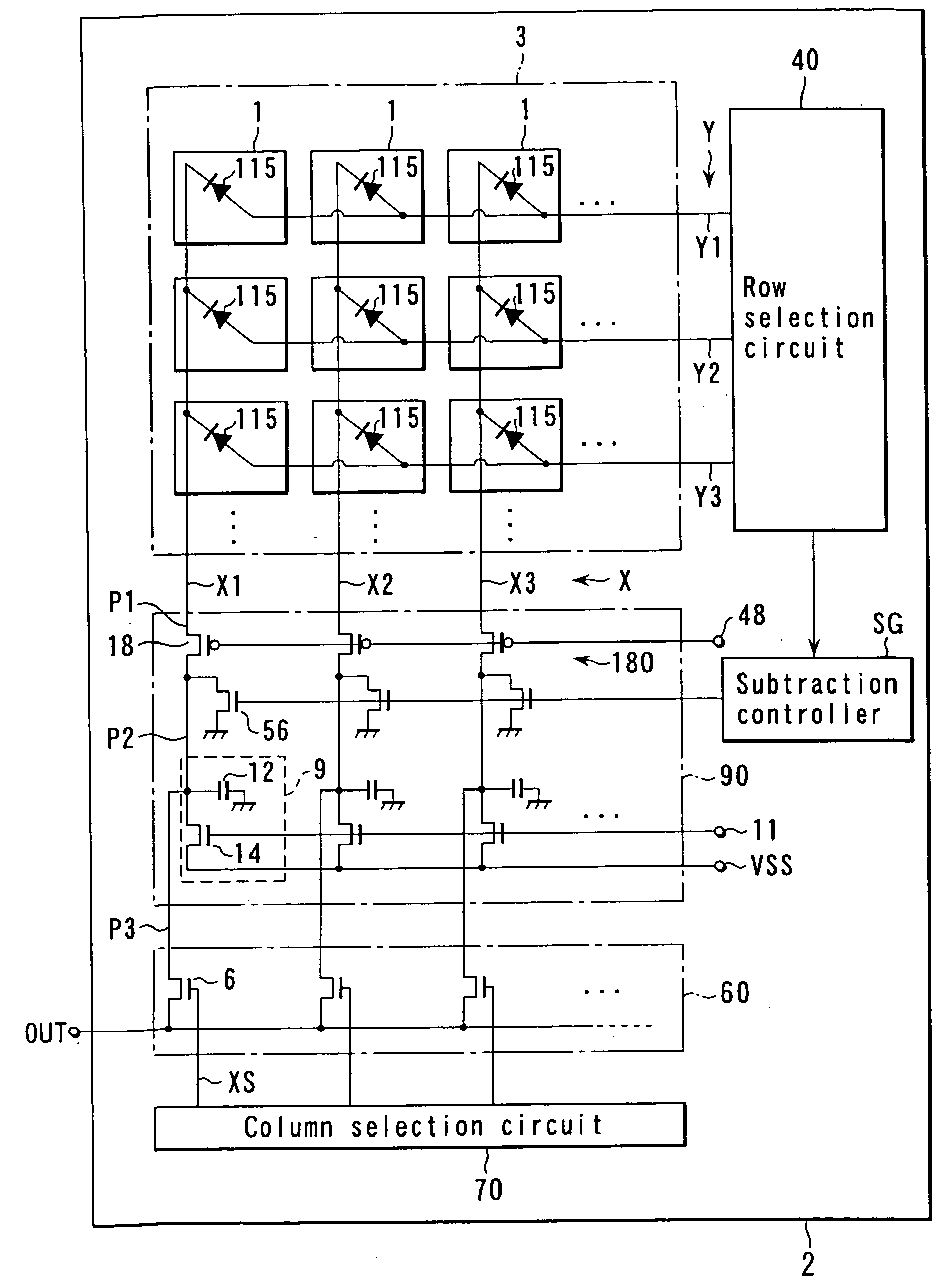
An uncooled solid-state infrared imager according to the present invention will be described below. FIG. 1 shows the whole configuration of the uncooled infrared sensor. As shown in FIG. 1, in the uncooled solid-state infrared imager, a signal line potential stabilizing circuit 180 for stabilizing the potential of each signal line X into a constant level is provided instead of the constant current source 80. Components similar to those shown in FIG. 17 are represented by same reference numerals in FIG. 1, and the descriptions thereof are simplified or omitted. In the subsequent embodiments, the similar components are represented by the same numerals and the descriptions thereof are simplified or omitted as well.

The uncooled solid-state infrared imager shown in FIG. 1 operates in substantially the same manner as those in FIGS. 15 and 17, except that the potential stabilizing circuit 180 provides a constant voltage biased current readout system in which the temperature information of...

third embodiment

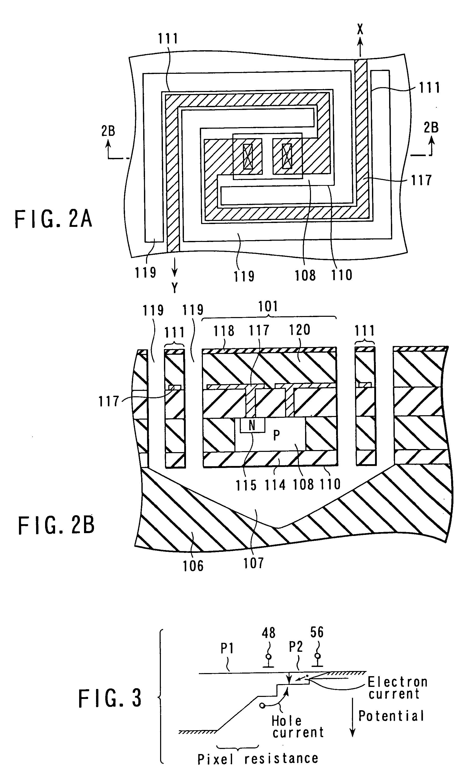
the potential of the node P2 becomes the same as that input from the voltage terminal RF to the (+) input terminal 32. Therefore, the operational amplifiers 30 serve as the signal line potential stabilizing circuit 180. Therefore, it is possible to completely prevent the negative feedback to the signal line potential caused when a load resistor is used as a simple circuitry for current voltage conversion. Furthermore, since the operational amplifier 30 performs voltage amplification, it is unnecessary to increase a resistance of the load resistor RL, and it is possible to remarkably reduce thermal noise as random noise generated in the load resistor.

FIG. 8 shows a first modification of the column amplifier 9 shown in FIG. 6. In this modification, the column amplifier 9 includes two inverter circuits 36A and 36B which are connected in series at a stage behind the operational amplifier 30, and each of which has a CMOS structure of p- and n-channel MOS transistors as shown in FIG. 9. T...

fourth embodiment

the non-sensing pixels 501 and the infrared sensing pixels 1 are formed in the common semiconductor substrate 2. Therefore, the temperature of the non-sensing pixel 501 changes due to the self-heating effect in substantially the same tendency as the temperature change of the infrared sensing pixel 1, and a current caused by self-heating flows in the signal line Xn+1. A self-heating component is the major part of the signal current in each of the signal lines X1 to Xn. With current removal circuit which is formed of the n MOS transistors 56 of the column amplification circuit 90 and the MOS transistor 57, a bias current component including the self-heating component is effectively cancelled without requiring any circuit-tuning of voltage or the like. More specifically, each MOS transistor 56 subtracts a bias current component including the self-heating component from the current flowing in a corresponding one of the signal lines X1 to Xn by the control of a voltage generated by the s...


PUM


Abstract

A solid-state infrared imager comprises a matrix array of infrared sensing pixels which are formed as an imaging area on a semiconductor substrate and each of which contains a pn-junction thermoelectric converter element to sense incident infrared radiation, row selection lines each connected to the pixels of a corresponding row, signal lines each connected to the pixels of a corresponding column, a row selection circuit which selects and drives one of the row selection lines, and a signal readout circuit which reads out signal currents output to the signal lines from the pixels corresponding to the row selection line driven by the row selection circuit. Particularly, the signal readout circuit includes a signal line potential stabilizer which stabilizes the potential of the signal line to a constant level, and a current-voltage converter which converts the signal current flowing in a signal line to a signal voltage.

Description

CROSS-REFERENCE TO RELATED APPLICATIONS This application is based upon and claims the benefit of priority from the prior Japanese Patent Application No. 2001-295106 filed Sep. 26, 2001, the entire contents of which are incorporated herein by reference. BACKGROUND OF THE INVENTION 1. Field of the Invention The present invention generally relates to a solid-state infrared imager, and more particularly to an uncooled or thermal solid-state infrared imager having an improved signal-readout structure. 2. Description of the Related Art An infrared imager is capable of capturing the image of an object without any distinction between night and day, and is advantageous in that the image is captured using infrared radiation whose penetration in smoke or fog is higher than that of visible radiation and in that temperature information of the object is also obtained. Therefore, the imager is widely applicable to defense systems, surveillance cameras, fire detection cameras, and the like. C...

Claims


Application Information

Patent Timeline
Patent Type & Authority Applications(United States)
IPC IPC(8): H01L27/14H01L27/146H04N5/33H04N5/335H04N5/355H04N5/357H04N5/369H04N5/374
CPCH04N5/33H01L27/14649
Inventor IIDA, YOSHINORISHIGENAKA, KEITAROMASHIO, NAOYA
Owner KK TOSHIBA
Why Eureka
Try Eureka