
Solid-state imaging device and electronic device

A solid-state image pickup, pixel technology, used in image communication, signal generators with a single pickup device, TV, etc., to achieve the effect of high sensitivity characteristics and good pixel characteristics

Active Publication Date: 2014-12-10
SONY SEMICON SOLUTIONS CORP
View PDF2 Cites 8 Cited by
  • Summary
  • Abstract
  • Description
  • Claims
  • Application Information

AI Technical Summary

Problems solved by technology

However, a three-transistor pixel that does not include a select transistor can be used for miniaturization of the pixel

Method used


Image

  • Solid-state imaging device and electronic device
  • Solid-state imaging device and electronic device
  • Solid-state imaging device and electronic device

Examples


no. 1 example

[0031] 1. First embodiment: back-illuminated solid-state image pickup unit

no. 2 example

[0032] 2. Second embodiment: front-illuminated solid-state image pickup unit

[0033] 3. Various modification examples

[0034] 4. Construction example of electronic equipment (application example)

[0035] (1. First embodiment)

[0036] First, before describing the configuration of the solid-state image pickup unit according to the first embodiment of the present disclosure, the influence of the sensitivity difference of the green pixel and the sensitivity difference between the blue pixel and the red pixel, which can be applied to the image pickup of the solid-state image pickup unit, will be briefly described. performance.

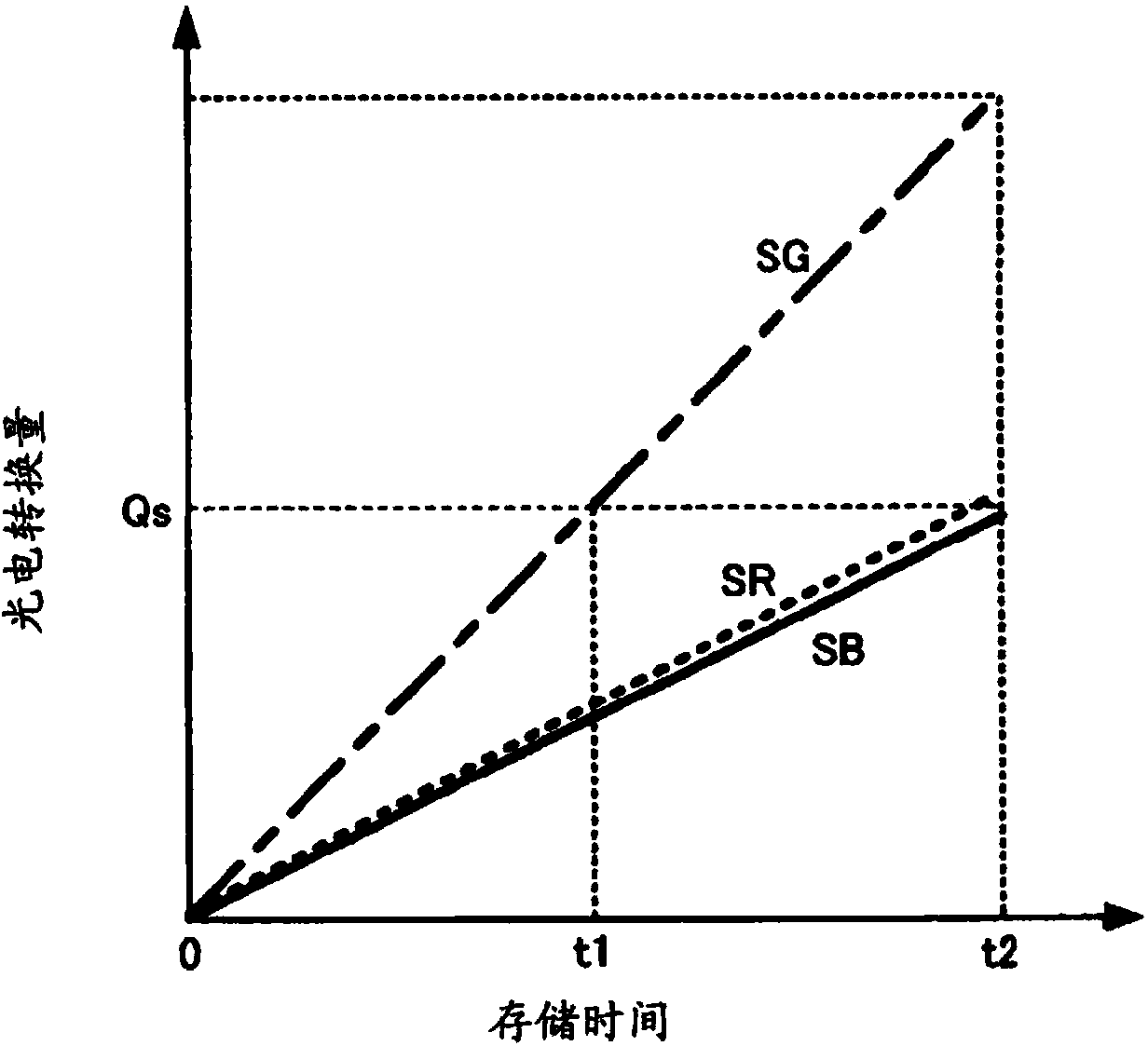
[0037] figure 1 Sensitivity characteristics of green pixels, blue pixels, and red pixels are shown. It should be noted that figure 1The horizontal axis and the vertical axis of each pixel sensitivity characteristic shown represent the charge storage time and the photoelectric conversion amount, respectively. and, figure 1 The characteristic (SB) ...

example 1

[0150] In the various embodiments described above, an example in which two green charge storage portions are provided in the green pixel 30 along the thickness direction of the substrate 50 is described; however, the present disclosure is not limited thereto. Three or more green charge storage portions may be provided in the green pixel 30 along the thickness direction of the substrate 50, and even in this case, effects similar to those of the above-described various embodiments are allowed to be obtained.


PUM


Abstract

This solid-state imaging device is provided with: a substrate (50); and a red pixel (10) having a red charge storage portion (11), a blue pixel (20) having a blue charge storage portion (21), and a green pixel (30) having a plurality of green charge storage portions (31a, 31b), said pixels being provided within the substrate (50). The plurality of green charge storage portions (31a, 31b) are arranged within the substrate (50) in the thickness direction of the substrate (50).

Description

technical field [0001] The present disclosure relates to a solid-state image pickup unit and electronic equipment including the solid-state image pickup unit. Background technique [0002] In recent years, as a solid-state image pickup unit (solid-state image pickup unit), a CMOS (Complementary Metal Oxide Semiconductor) image sensor has been used in various applications for replacing a CCD (Charge Coupled Device). For example, the number of cases where CMOS image sensors are used as solid-state image pickup units mounted in digital cameras, digital camcorders, surveillance cameras, cameras for broadcasting, movie production, or commercial use or built in mobile phones is increasing camera in . This is because, in addition to higher pickup speed (higher frame rate) and lower power consumption, etc., the image quality of the CMOS image sensor is remarkably improved compared with the CCD. Also, the CMOS image sensor is advantageous in that pixel portions of unit pixels (here...

Claims


Application Information

Patent Timeline
Patent Type & Authority Applications(China)
IPC IPC(8): H01L27/146H04N5/374H04N9/07H04N23/12
CPCH01L27/1464H01L27/14647H01L27/14638H01L27/14641H01L27/14609H01L27/14603H01L27/14612H01L27/14627H01L27/14636H01L27/14645
Inventor 石渡宏明
Owner SONY SEMICON SOLUTIONS CORP
Learn More