NAND flash memory device and method of manufacturing the same

Inactive Publication Date: 2007-01-04
SK HYNIX INC
View PDF13 Cites 4 Cited by
  • Summary
  • Abstract
  • Description
  • Claims
  • Application Information

AI Technical Summary

Benefits of technology

[0007] An embodiment of the present invention provides a NAND flash memory device and a method of

Problems solved by technology

However, these materials tend to have a high leakage current at a high voltage

Method used


Image

  • NAND flash memory device and method of manufacturing the same
  • NAND flash memory device and method of manufacturing the same
  • NAND flash memory device and method of manufacturing the same

Examples


Embodiment Construction

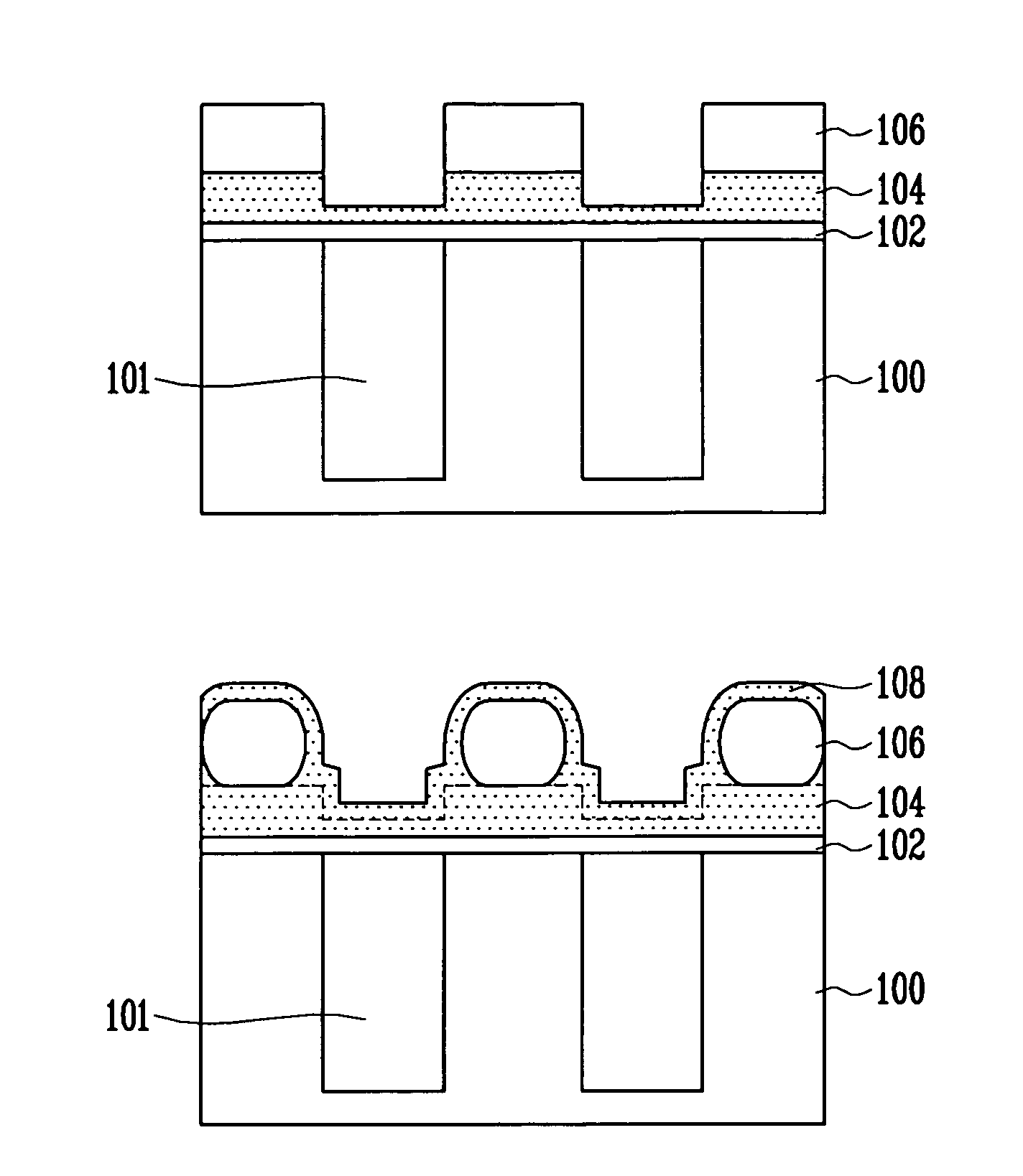
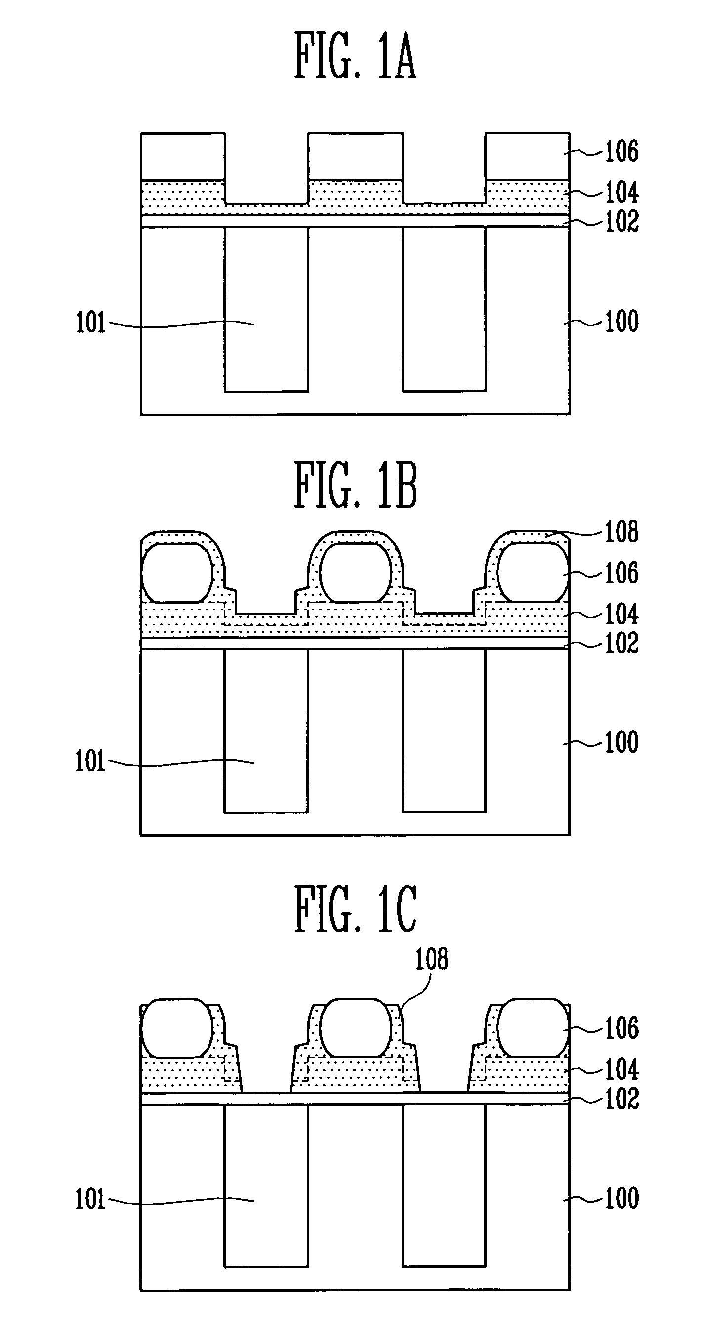
[0013] Referring to FIG. 1a, a tunnel oxide film (or tunnel dielectric film) 102, a first conductive film 104 for the floating gate, and a first hard mask film 106 are sequentially formed on a semiconductor substrate 100 in which isolation structures 101 are formed. The first hard mask film 106 may be formed to a thickness of 500 Å to 6000 Å using a nitride film and the first conductive film 104 may be formed using a polysilicon film.

[0014] The first hard mask film 106 and a part of the first conductive film 104 are etched. One of the following methods may be used: (1) etching only the first hard mask film 106; (2) etching the first conductive film 104 so that the first conductive film 104 having a thickness of about 50 Å to 100 Å remains on the tunnel oxide film 102; or (3) etching the first conductive film 104 until the tunnel oxide film 102 is exposed. In the present implementation, the etch method (2) is used.

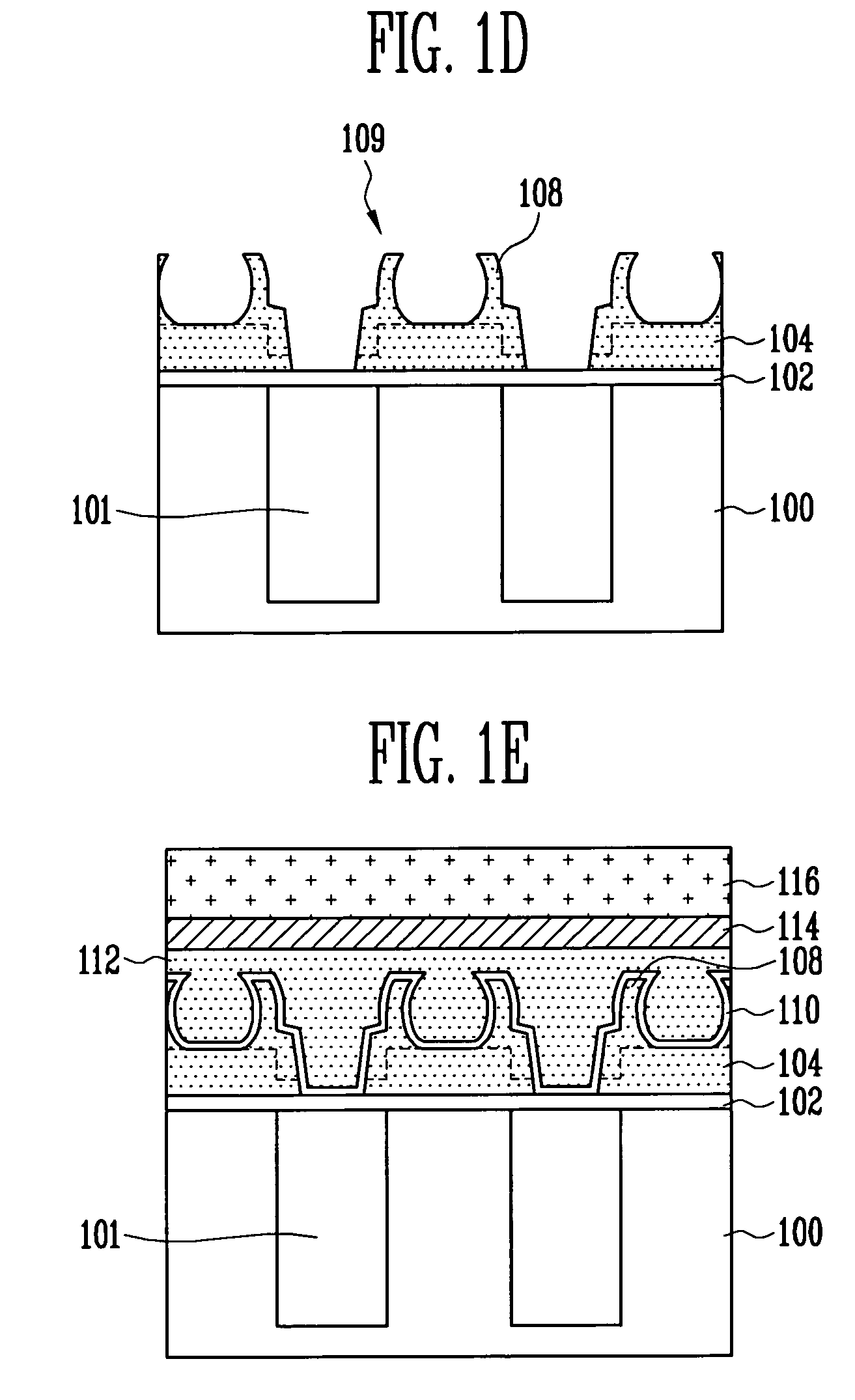
[0015] Referring to FIG. 1b, the corners of the first hard mask film...


PUM


Abstract

A method of manufacturing a non-volatile memory device includes forming a first conductive layer over a tunnel dielectric layer that is provided on a semiconductor substrate. A non-conductive layer is formed over the first conductive film. The non-conductive layer is etched to define a stack structure between first and second trenches, the stack structure including the first conductive layer and the non-conductive layer. A second conductive layer is formed over the stack structure and into the first and second trenches. An upper portion of the second conductive layer is etched to expose the non-conductive layer of the stack structure. The non-conductive layer of the stack structure is removed to form a three-dimensional (3-D) floating gate with an opening, the floating gate including the first and second conductive layers. A third conductive layer is provided within the 3-D floating gate via the opening of the 3-D floating gate to form a control gate.

Description

BACKGROUND [0001] The present invention relates to a flash memory device, and more particularly, to a NAND flash memory device and a method of manufacturing the same, in which the program speed can be increased by enlarging the surface area of the floating gate. [0002] A conventional flash memory device is formed by sequentially forming a tunnel oxide film, a conductive film for a floating gate, a dielectric film, and a conductive film for a control gate on a semiconductor substrate in which an isolation film is formed. [0003] With the continuously decreasing line width of devices a method of forming a flash memory device using a Self-Aligned Floating Gate (hereinafter, referred to as “SAFG”) has been developed. The method of forming the flash memory device using SAFG will be described in short below. [0004] A tunnel oxide film, a first polysilicon film, and a pad nitride film are sequentially formed on a semiconductor substrate. The pad nitride film, the first polysilicon film, the...

Claims


Application Information

Patent Timeline
IPC IPC(8): H01L21/8232H01L21/335
CPCH01L21/28273H01L27/105H01L29/42324H01L27/11521H01L27/11551H01L27/11519H01L29/40114H10B41/10H10B41/20H10B41/30
Inventor CHOI, EUN SEOKKIM, NAM KYEONG
Owner SK HYNIX INC
Why Eureka
Try Eureka