
AlGaN/GaN schottky diode with Al component gradually changed and preparation method thereof

A Schottky diode and diode technology, applied in the field of microelectronics, can solve the problems that the concentration of two-dimensional electron gas is not high enough, and is not suitable for higher frequency and larger current working conditions, so as to reduce material stress, increase concentration, and improve The effect of device speed

Inactive Publication Date: 2018-09-11
XIDIAN UNIV
View PDF3 Cites 5 Cited by
  • Summary
  • Abstract
  • Description
  • Claims
  • Application Information

AI Technical Summary

Problems solved by technology

[0004] In 1999, Gaska R and others grew AlGaN / GaN heterostructures with an Al composition of 0.2 on sapphire substrates, 6H-SiC and 4H-SiC substrates by means of modulation doping, and measured and calculated the two Two-dimensional electron gas concentration and corresponding mobility, see Electron Mobility in Modulation-doped AlGaN-GaN Heterostructures[J].Appl Phys Lett,1999,74(2):2872289. Although the two-dimensional electron gas concentration of this method can reach 10 13 cm-3, but because its Al composition is fixed at 0.2, the two-dimensional electron gas concentration is not high enough to be suitable for higher frequency and larger current working conditions

Method used


Image

  • AlGaN/GaN schottky diode with Al component gradually changed and preparation method thereof
  • AlGaN/GaN schottky diode with Al component gradually changed and preparation method thereof

Examples


Embodiment 1

[0029] Example 1, the preparation of heavily doped n-type concentration is 10 18 cm -3 , the lightly doped n-type concentration is 10 14 cm -3 Graded Al composition AlGaN / GaN Schottky diodes.

[0030] Step one, heat treatment.

[0031] After the sapphire substrate was polished and cleaned, it was placed in the metal organic chemical vapor deposition MOCVD reaction chamber, and the vacuum degree of the reaction chamber was reduced to 2×10 -2 Torr;

[0032] Introduce hydrogen gas into the reaction chamber, and under the condition that the pressure of the MOCVD reaction chamber reaches 20 Torr, the substrate is heated to a temperature of 1200° C. and kept for 10 minutes to complete the heat treatment of the substrate.

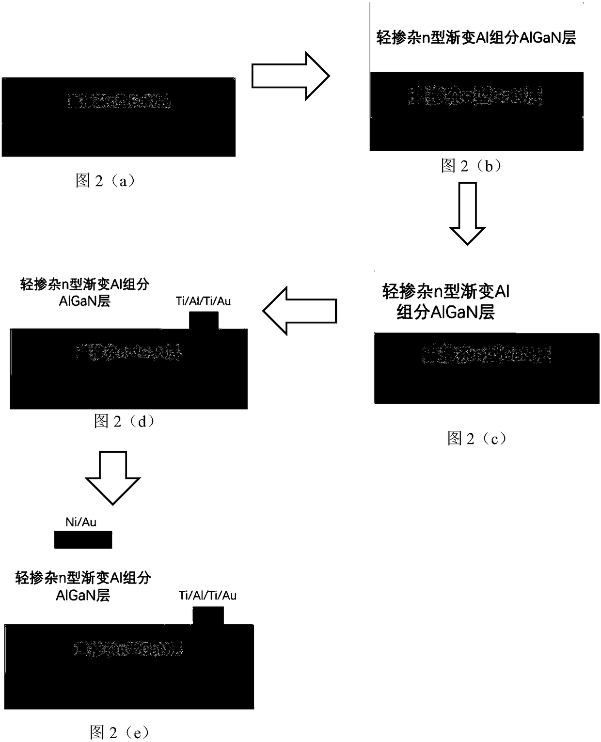
[0033] Step 2, growing a heavily doped n-type non-polar GaN layer, as shown in Figure 2(a).

[0034] The MOCVD process was adopted on the sapphire substrate. Under the condition of the reaction chamber temperature of 1000°C, the ammonia gas with a flow rate ...

Embodiment 2

[0042] Example 2, the preparation of heavily doped n-type concentration is 10 20 cm -3 , the lightly doped n-type concentration is 10 16 cm -3 Graded Al composition AlGaN / GaN Schottky diodes.

[0043] Step 1, heat treatment.

[0044] The specific implementation of this step is the same as step 1 of Embodiment 1.

[0045] Step 2, growing a heavily doped n-type non-polar GaN layer, as shown in Figure 2(a).

[0046] The MOCVD process is adopted on the sapphire substrate, and the temperature of the reaction chamber is set to 1100°C. At the same time, ammonia gas with a flow rate of 3000 sccm, a gallium source with a flow rate of 200 sccm, and a silicon source with a flow rate of 80 sccm are introduced into the reaction chamber. A heavily doped n-type non-polar GaN layer with a thickness of 2 μm was grown under the conditions, in which the silicon doping concentration was 10 20 cm -3 .

[0047] Step 3, growing a lightly doped n-type graded Al composition AlGaN layer.

[00...

Embodiment 3

[0054] Example 3, the preparation of heavily doped n-type concentration is 10 19 cm -3 , the lightly doped n-type concentration is 10 15 cm -3 Graded Al composition AlGaN / GaN Schottky diodes.

[0055] Step A, heat treatment.

[0056] The specific implementation of this step is the same as step 1 of Embodiment 1.

[0057] Step B, growing a heavily doped n-type non-polar GaN layer, as shown in Figure 2(a).

[0058] Place the heat-treated sapphire substrate in the reaction chamber, heat the reaction chamber to 1080°C, and simultaneously feed ammonia gas with a flow rate of 2500 sccm, a gallium source with a flow rate of 150 sccm, and a silicon source with a flow rate of 70 sccm, at a pressure of 40 Torr Under the conditions of growth thickness of 3 μm and silicon doping concentration of 10 19 cm -3 A heavily doped n-type nonpolar GaN layer.

[0059] Step C, growing a lightly doped n-type graded Al composition AlGaN layer.

[0060] C1) Place the substrate grown on the hea...


PUM

PropertyMeasurementUnit
Thicknessaaaaaaaaaa
Doping concentrationaaaaaaaaaa
Thicknessaaaaaaaaaa

Abstract

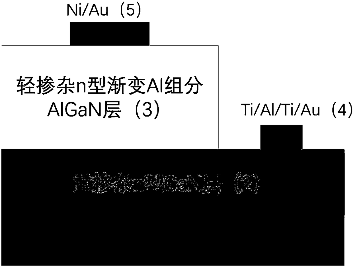
The invention discloses a preparation method of an AlGaN / GaN heterojunction schottky barrier diode with an Al component gradually changed and mainly aims at solving the problem that an existing schottky diode is low in two-dimensional electron gas concentration. The AlGaN / GaN heterojunction schottky barrier diode with the Al component gradually changed comprises a substrate, a heavily doped n typenon-polar GaN epitaxial layer and a lightly doped n type AlGaN layer from bottom to top, wherein an ohmic contact electrode made from a metal Ti / Al / Ti / Au material is arranged on the heavily doped n type non-polar GaN epitaxial layer, and a schottky contact electrode made from a metal Ni / Au material is arranged on a lightly doped n type gradually changed Al component AlGaN layer. The schottky barrier diode is characterized in that the Al component in the lightly doped n type AlGaN layer is nonlinearly changed from 0.01 to 1 from down to up. The schottky barrier diode disclosed by the inventionis increased in the two-dimensional electron gas concentration at a heterojunction of a schottky diode, so as to increase the speed of a device, and can be used as a high-frequency, low-voltage and heavy-current rectification diode or a small signal wave detecting diode.

Description

technical field [0001] The invention belongs to the technical field of microelectronics, and in particular relates to a Schottky diode with high carrier mobility, which can be used as a high-frequency, low-voltage, high-current rectifier diode or a small-signal detection diode. technical background [0002] A Schottky diode is a low-power, ultra-high-speed semiconductor device. Due to its low conduction voltage and no reverse recovery problem, it is widely used in switching power supplies, frequency converters, drives and other circuits, as high-frequency, low-voltage, high-current rectifier diodes or small-signal detection diodes. [0003] During the development of Schottky diodes, how to improve the carrier mobility of Schottky diodes has always been a key issue in improving device performance. In recent years, the two-dimensional electron gas produced by the heterojunction epitaxy process has significantly improved the mobility characteristics of the device, allowing car...

Claims


Application Information

Patent Timeline
IPC IPC(8): H01L29/872H01L29/205H01L21/329
CPCH01L29/872H01L29/205H01L29/66212
Inventor 许晟瑞王学炜郝跃张进成毕臻艾丽霞李文吕玲
Owner XIDIAN UNIV
Learn More