

Organic light emitting diode display device and method of driving the same
- Summary
- Abstract
- Description
- Claims
- Application Information
AI Technical Summary
Benefits of technology
Problems solved by technology
Method used
Image

Examples
first embodiment
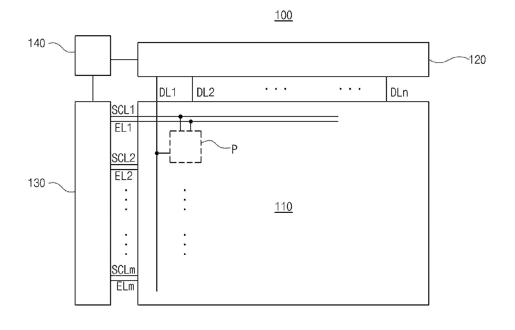
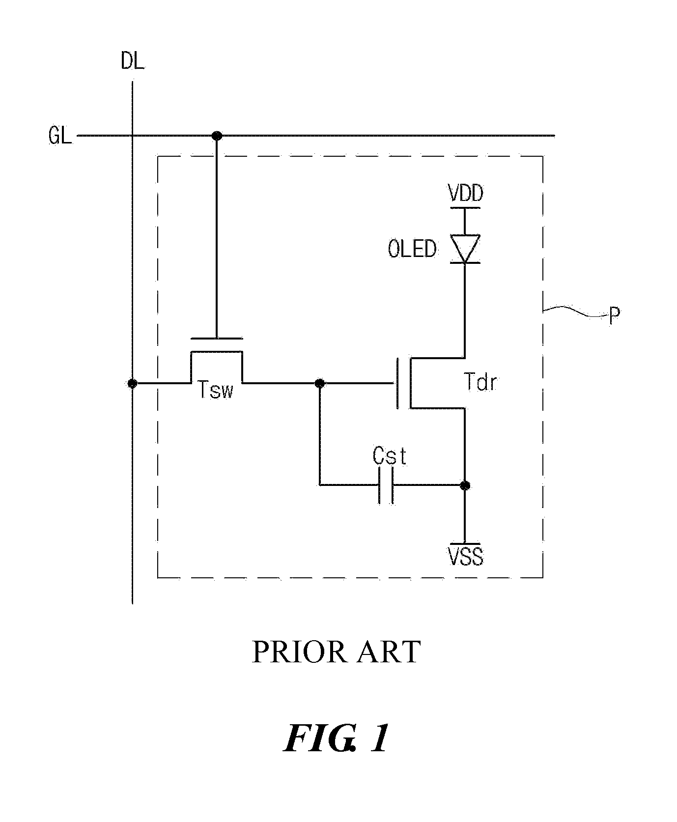
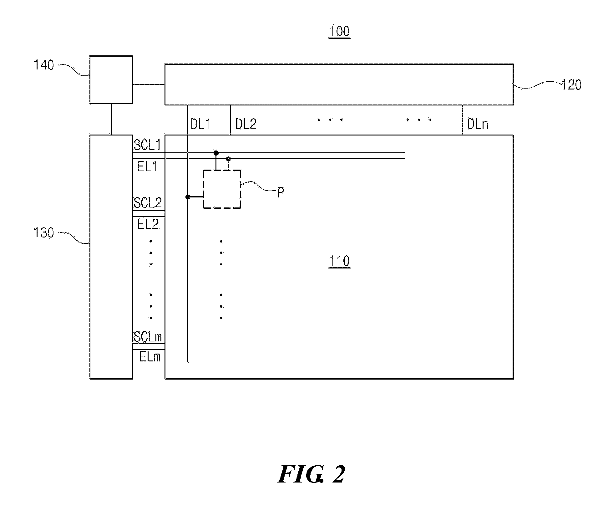
[0046]FIG. 2 is a schematic diagram of an organic light emitting diode (OLED) display device according to an embodiment of the present invention, and FIG. 3 is a schematic equivalent circuit diagram of an OLED display device according to the present invention.
[0047]As shown in FIG. 2, an OLED display device 100 according to the present invention may include a display panel 110 configured to display images, a source driver 120, a scan driver 130, and a timing controller 140 configured to control a driving time point of each of the source driver 120 and the scan driver 130.
[0048]The display panel 110 may include a plurality of scan lines SCL1 to SCLm and a plurality of data lines DL1 to DLn, which may intersect one another to define a plurality of pixel regions P, and a plurality of emission control lines EL1 to ELm.
[0049]Since the respective pixel regions P have the same configuration, the plurality of scan lines SCL1 to SCLm, the plurality of data lines DL1 to DLn, and the plurality...
second embodiment
[0127]In a pixel structure of the OLED display device according to the present invention, a connection structure among first through third transistors T1 to T3 may be modified.
[0128]Source and gate electrodes of the first transistor T1 may be connected to a terminal of a high-potential voltage Vdd and an initialization line IL, respectively, and a drain electrode of the first transistor T1 may be connected to a second node N2.
[0129]The first transistor T1 may be turned on in response to an initialization signal applied through the initialization line IL, and apply the high-potential voltage Vdd to the second node N2. In this case, the high-potential voltage Vdd may be, for example, about 5 V.
[0130]Source and gate electrodes of the second transistor T2 may be connected to a third node N3 and a sensing line SEL, respectively, and a drain electrode of the second transistor T2 may be connected to a first node N1.
[0131]The second transistor T2 may be turned on in response to a sensing si...
third embodiment
[0189]In a pixel structure of the OLED display device according to the present invention, a connection structure among the switching transistor Tsw, the emission control transistor Tem, and the first through third transistors T1 to T3 may be modified.
[0190]Source and gate electrodes of the switching transistor Tsw may be connected to a data line DL and an (N+1)th scan line SCL(N+1), respectively, and a drain electrode of the switching transistor Tsw may be connected to a second node N2.
[0191]The switching transistor Tsw may be turned on in response to an (N+1)th scan signal applied through the (N+1)th scan line SCL(N+1), and apply a data voltage Vdata to the second node N2.
[0192]Source and gate electrodes of the emission control transistor Tem may be connected to a third node N3 and an (N+1)th emission control line EL(N+1), respectively, and a drain electrode of the emission control transistor Tem may be connected to one electrode of the OLED.
[0193]The emission control transistor Te...
PUM
 Abstract
Description
Claims
Application Information