
Image sensors and image processing devices including the same

a technology of image processing device and image sensor, which is applied in the direction of radio frequency control device, television system, instruments, etc., can solve the problem of reducing the area that a light receiving region takes in the entire pixel

Active Publication Date: 2013-06-06
SAMSUNG ELECTRONICS CO LTD
View PDF4 Cites 61 Cited by
  • Summary
  • Abstract
  • Description
  • Claims
  • Application Information

AI Technical Summary

Benefits of technology

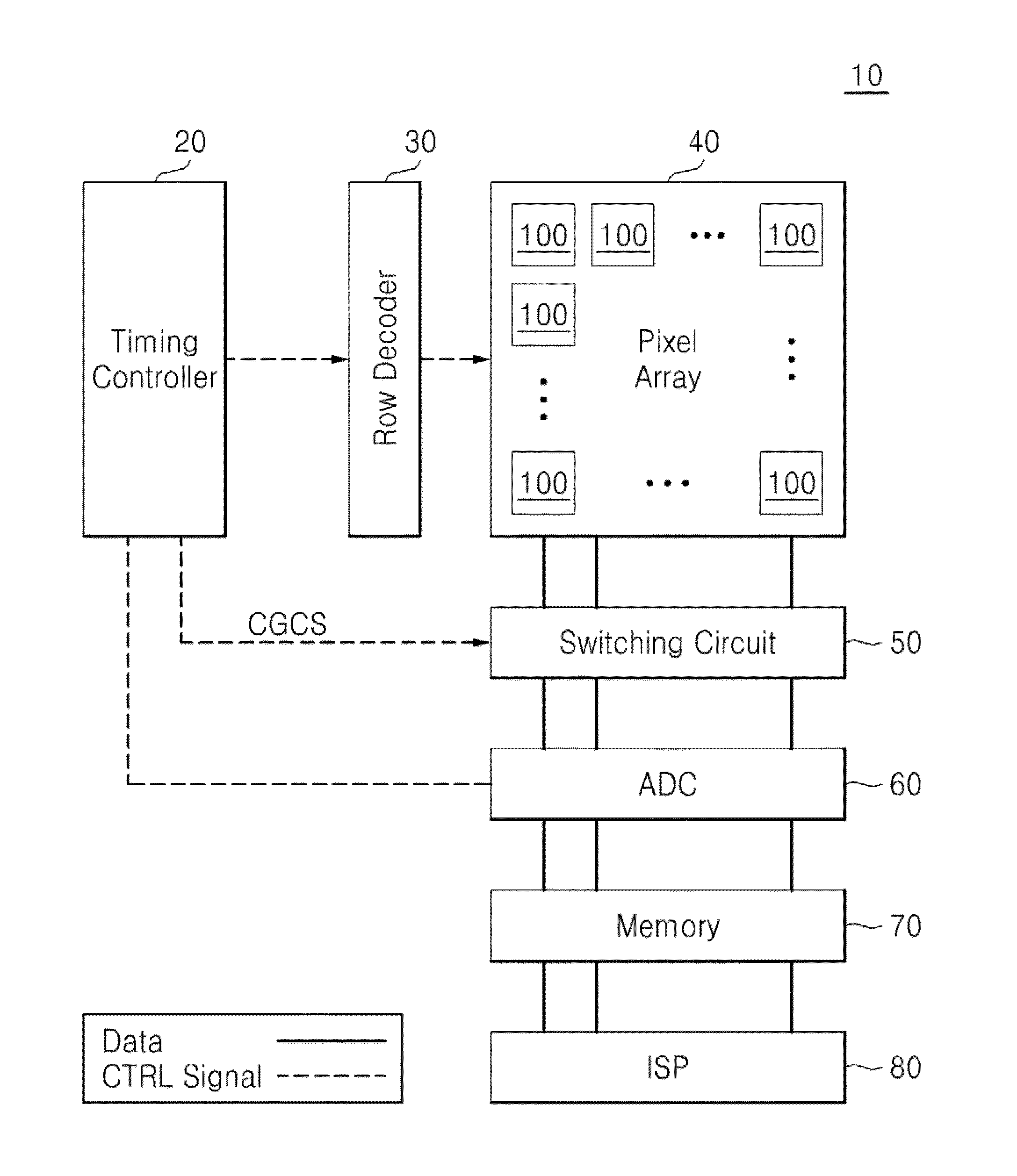
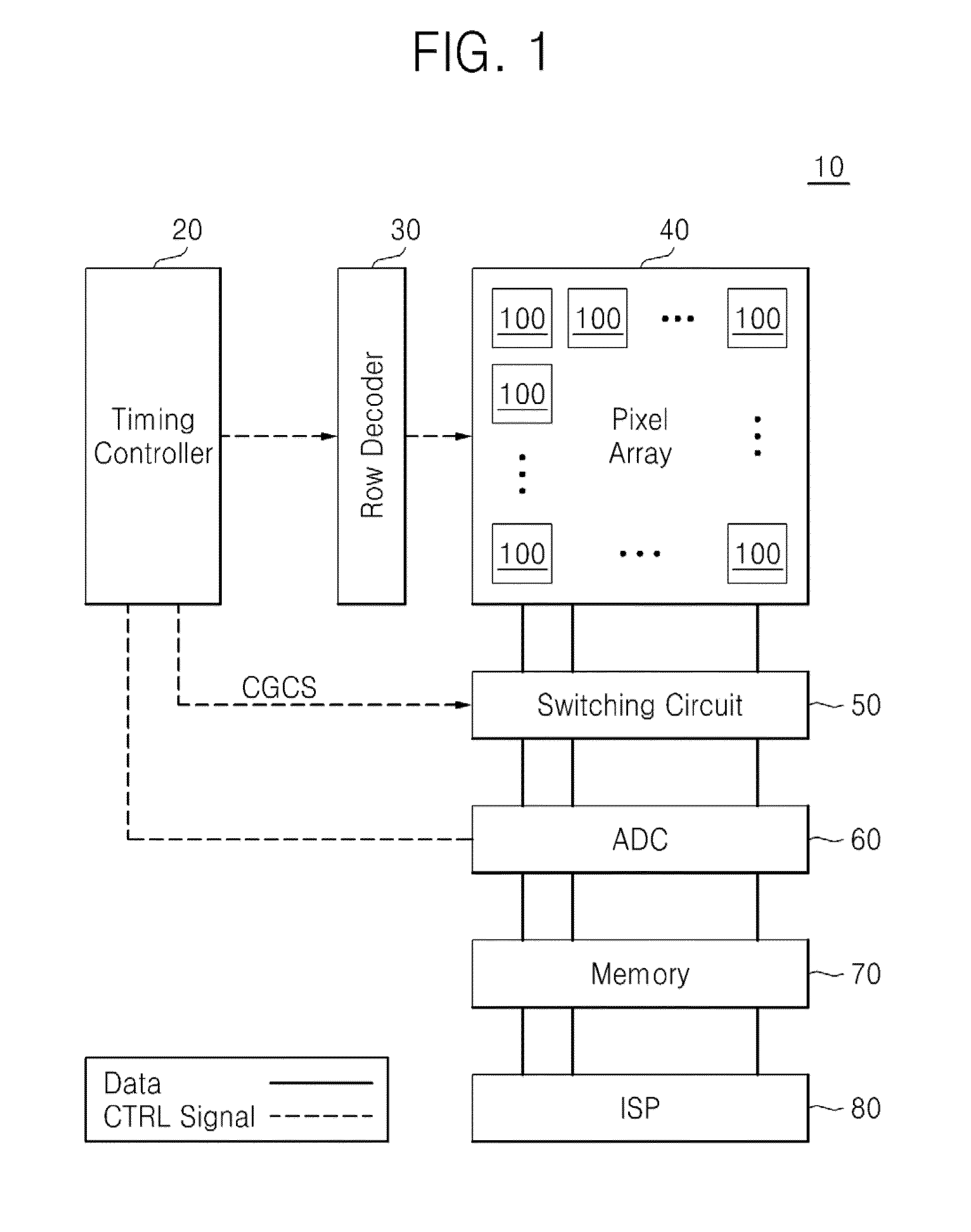
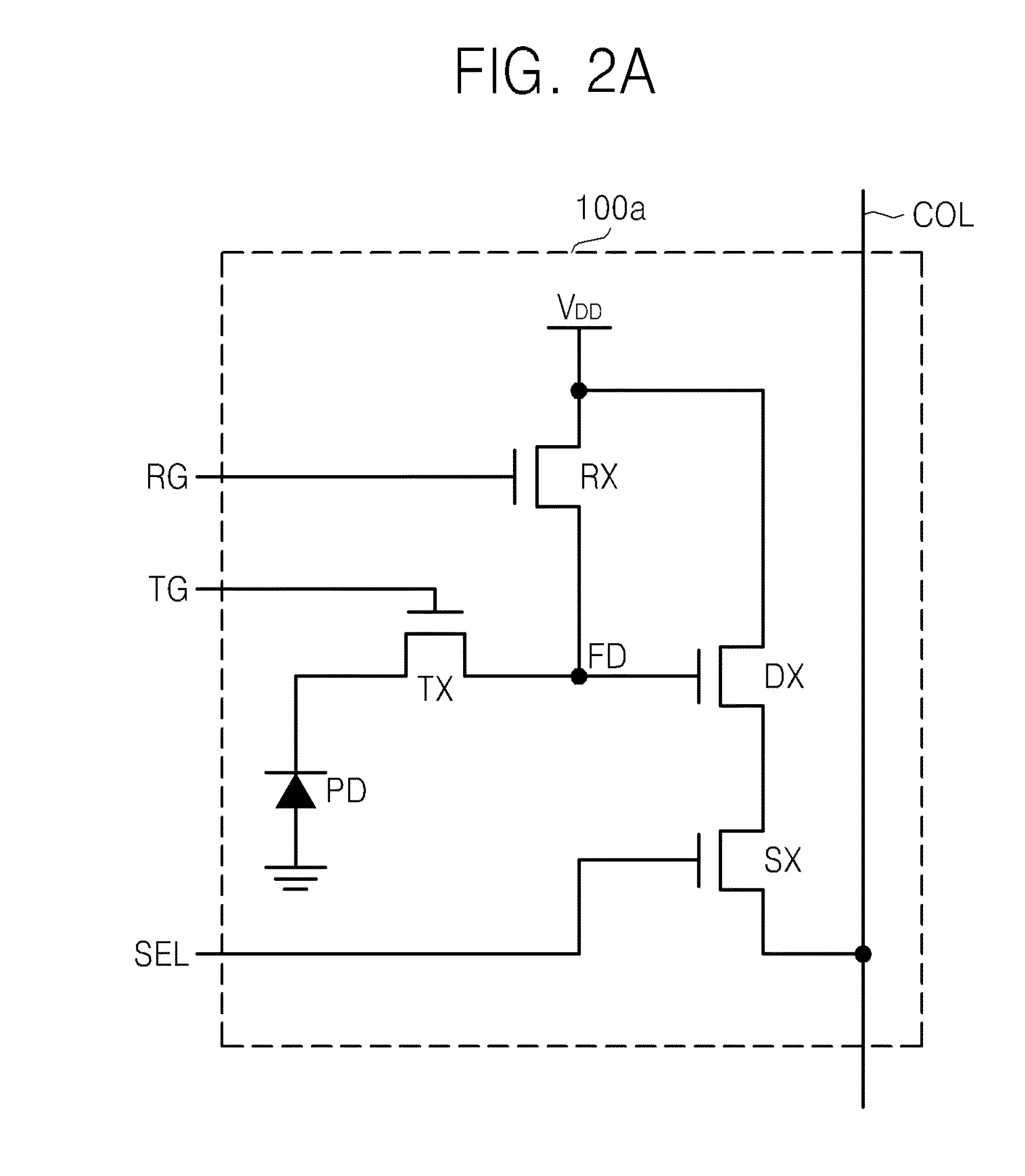
The patent describes an image sensor that includes a photodiode, a sensing node, a read-out circuit, and one or more capacitors. The conversion gain control line can be selectively connected to the ground or the output line based on a control signal. The image sensor can also include a switch and a timing controller to control the output of each pixel. The technical effect of this invention is to provide an image sensor with improved control over the conversion gain, which can adjust the sensitivity of pixels to optical signals and improve image quality.

Problems solved by technology

However, when additional elements are provided in a pixel to adjust the conversion gain, an area that a light receiving region takes in the entire pixel is reduced, which is inefficient.

Method used


Image

  • Image sensors and image processing devices including the same
  • Image sensors and image processing devices including the same
  • Image sensors and image processing devices including the same

Examples


Embodiment Construction

[0044]Example embodiments will now be described more fully with reference to the accompanying drawings. Embodiments, however, may be embodied in many different forms and should not be construed as being limited to the embodiments set forth herein. Rather, these example embodiments are provided so that this disclosure will be thorough and complete, and will fully convey the scope to those skilled in the art. In the drawings, the thicknesses of layers and regions may be exaggerated for clarity.

[0045]It will be understood that when an element is referred to as being “on,”“connected to,”“electrically connected to,” or “coupled to” to another component, it may be directly on, connected to, electrically connected to, or coupled to the other component or intervening components may be present. In contrast, when a component is referred to as being “directly on,”“directly connected to,”“directly electrically connected to,” or “directly coupled to” another component, there are no intervening c...


PUM


Abstract

An image sensor may include a photodiode configured to convert an optical signal into photogenerated charge, a sensing node adjacent to the photodiode and configured to sense the photogenerated charge, a read-out circuit configured to convert the photogenerated charge into an electrical signal and to output the electrical signal through an output line, and / or at least one capacitor formed between the sensing node and a conversion gain control line. The conversion gain control line corresponding to the at least one capacitor may be selectively connected to a ground line or the output line based on at least one control signal.

Description

CROSS-REFERENCE TO RELATED APPLICATION(S)[0001]This application claims priority from Korean Patent Application No. 10-2011-0128659, filed on Dec. 2, 2011, in the Korean Intellectual Property Office (KIPO), the entire contents of which are incorporated herein by reference.BACKGROUND[0002]1. Field[0003]Example embodiments may relate to image sensors and / or image processing devices including the same. Example embodiments also may relate to image sensors for adjusting conversion gains and / or image processing devices including the same.[0004]2. Description of Related Art[0005]A sensor including a pixel array, which senses effective physical quantity such as light intensity, temperature, mass, or time and outputs an electrical signal, is used in various areas. In particular, an image sensor measuring an image of a photographed object is applied to various fields. Conversion gain with which an optical signal is converted into an electrical signal is important in image sensors.[0006]It is n...

Claims


Application Information

Patent Timeline
Patent Type & Authority Applications(United States)
IPC IPC(8): H01L27/146H04N5/335H04N25/00
CPCH01L27/14609H04N5/37452H04N5/3745H04N5/3559H04N25/59H04N25/771H04N25/77H04N25/76
Inventor LIM, YONGLIM, MOO SUP
Owner SAMSUNG ELECTRONICS CO LTD
Learn More