Multilayer ceramic electronic component and method of manufacturing the same

a technology of ceramic electronic components and ceramic ceramics, applied in the direction of fixed capacitor details, stacked capacitors, fixed capacitors, etc., can solve the problems of limit to lowering equivalent series resistance and voltage noise, and achieve the effects of reducing a big-v phenomenon, increasing equivalent series resistance (esr), and increasing equivalent series inductance (esl)

Active Publication Date: 2013-06-06
SAMSUNG ELECTRO MECHANICS CO LTD
View PDF4 Cites 9 Cited by
  • Summary
  • Abstract
  • Description
  • Claims
  • Application Information

AI Technical Summary

Benefits of technology

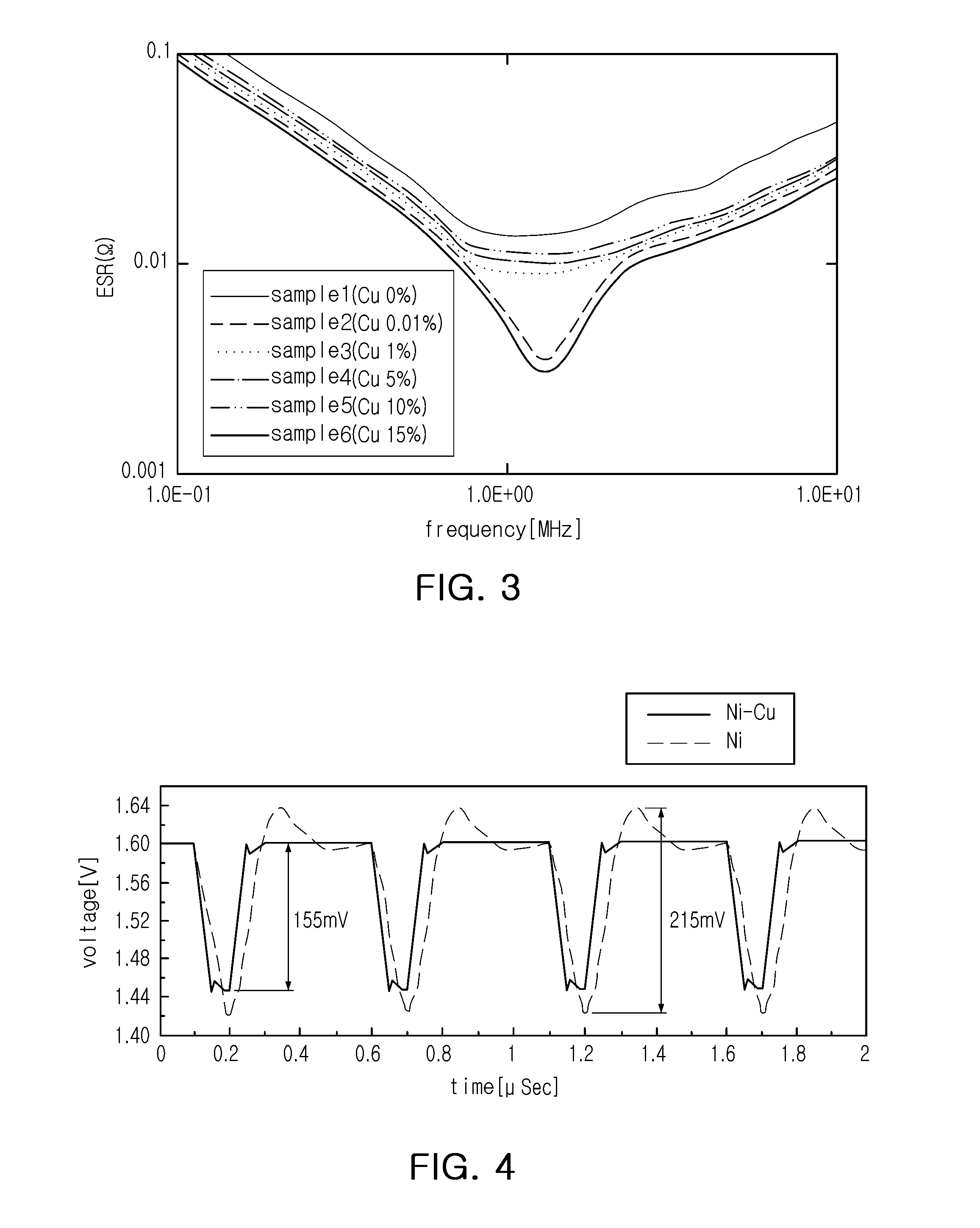
[0014]An aspect of the present invention provides a multilayer ceramic electronic component capable of reducing a Big-V phenomenon by increasing equivalent series resistance (ESR) without an increase in equivalent series inductance (ESL).

Problems solved by technology

Therefore, when decoupling capacitors having low equivalent series resistance (ESR) are connected in parallel, deviation from the target impedance |Z| at a specific frequency, the so-called “Big-V” phenomenon, may occur, resulting in voltage noise.
Therefore, although equivalent series inductance (ESL) needs to be lowered in the case of decoupling capacitors, there may be a limit to lowering equivalent series resistance (ESR), because it is necessary to reduce the Big-V phenomenon due to low equivalent series resistance (ESR).

Method used

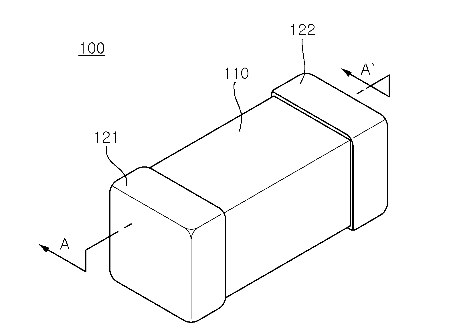
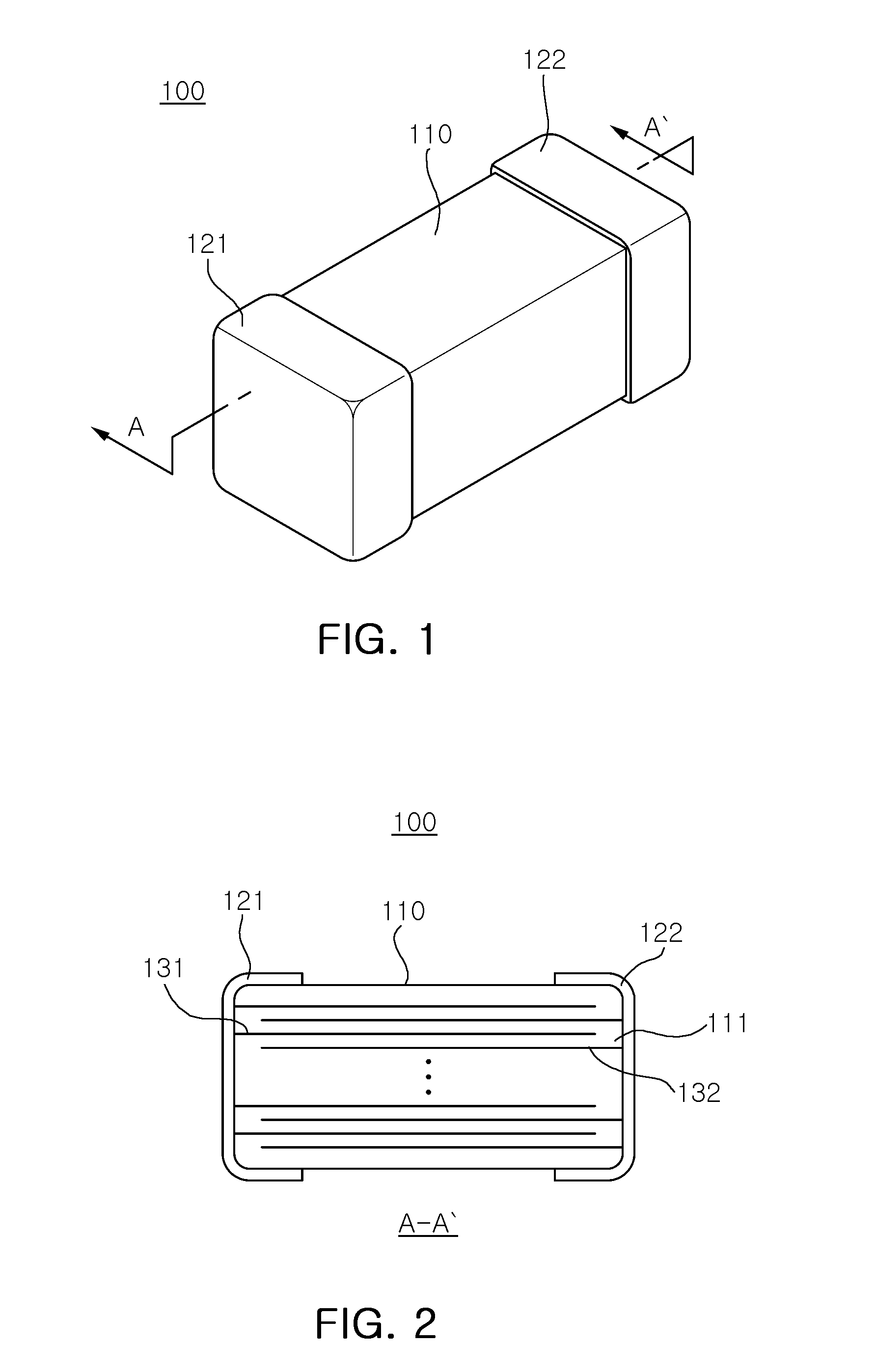

Image

  • Multilayer ceramic electronic component and method of manufacturing the same
  • Multilayer ceramic electronic component and method of manufacturing the same
  • Multilayer ceramic electronic component and method of manufacturing the same

Examples


Embodiment Construction

[0032]Hereinafter, embodiments of the present invention will be described in detail with reference to the accompanying drawings so that they can be easily practiced by those skilled in the art to which the present invention pertains.

[0033]However, the invention may be embodied in many different forms and should not be construed as being limited to the embodiments set forth herein.

[0034]The embodiments of the present invention are provided so that those skilled in the art may more completely understand the present invention.

[0035]In the drawings, the shapes and dimensions may be exaggerated for clarity, and the same reference numerals will be used throughout to designate the same or like components.

[0036]In addition, like reference numerals denote parts performing similar functions and actions throughout the drawings.

[0037]In addition, unless explicitly described otherwise, 1“comprising” any components will be understood to imply the inclusion of other components but not the exclusio...


PUM

PropertyMeasurementUnit
particle sizeaaaaaaaaaa
capacitanceaaaaaaaaaa
sizeaaaaaaaaaa

Abstract

There is provided a multilayer ceramic electronic component, including: a ceramic element having a plurality of dielectric layers laminated therein; and first and second internal electrodes formed within the ceramic element, wherein the first and second internal electrodes include 80 to 99.98 wt % of nickel (Ni), 0.01 to 10 wt % of copper (Cu), and 0.01 to 10 wt % of barium titanate (BaTiO3).

Description

CROSS-REFERENCE TO RELATED APPLICATIONS[0001]This application claims the priority of Korean Patent Application No. 10-2011-0129650 filed on Dec. 6, 2011, in the Korean Intellectual Property Office, the disclosure of which is incorporated herein by reference.BACKGROUND OF THE INVENTION[0002]1. Field of the Invention[0003]The present invention relates to a multilayer ceramic electronic component and a method of manufacturing the same.[0004]2. Description of the Related Art[0005]Electronic parts using a ceramic material include a capacitor, an inductor, a piezoelectric element, a varistor, a thermistor, or the like.[0006]Among these ceramic electronic parts, a multi-layer ceramic capacitor (MLCC) may have advantages such as a small size, high capacity, and easy mounting thereof.[0007]A multilayer ceramic capacitor is a chip type condenser having a main function of being charged with or discharging electricity while being mounted on a circuit board used in a variety of electronic produc...

Claims


Application Information

Patent Timeline
Patent Type & Authority Applications(United States)
IPC IPC(8): H01G4/008H05K3/00
CPCH01G4/30H01G4/0085Y10T29/435Y10T29/49124H01G4/12
Inventor HWANG, SEOK JOONKIM, JE JUNGCHOI, JAE YEOLKWON, SANG HOON
Owner SAMSUNG ELECTRO MECHANICS CO LTD
Why Eureka
Try Eureka