Supercharge Your Innovation With Domain-Expert AI Agents!

Semiconductor device having plural semiconductor chips

a semiconductor chip and semiconductor technology, applied in the field of semiconductor devices, can solve problems such as inability to direct electrical conta

Inactive Publication Date: 2013-06-20
LONGITUDE SEMICON S A R L
View PDF4 Cites 8 Cited by
  • Summary
  • Abstract
  • Description
  • Claims
  • Application Information

AI Technical Summary

Benefits of technology

The semiconductor device described in this patent has two chips stacked together. The first chip has first and second terminals, while the second chip has third and fourth terminals. The first chip's internal node changes its electrical potential in response to the first terminal's potential. The second chip's internal node changes its electrical potential in response to the third and fourth terminals' potential. By connecting these internal nodes, the chips can communicate with each other. This design allows for more efficient data transfer between the chips.

Problems solved by technology

In other words, there has conventionally been a problem that input terminals that are connected to input terminals of other chips and therefore not capable of direct electrical contact and are not subjected to the boundary scan test method cannot be tested whether electrically connected to outside.

Method used


Image

  • Semiconductor device having plural semiconductor chips
  • Semiconductor device having plural semiconductor chips
  • Semiconductor device having plural semiconductor chips

Examples


Embodiment Construction

[0021]Hereinafter, a preferred embodiment of the present invention will be described in detail with reference to the accompanying drawings.

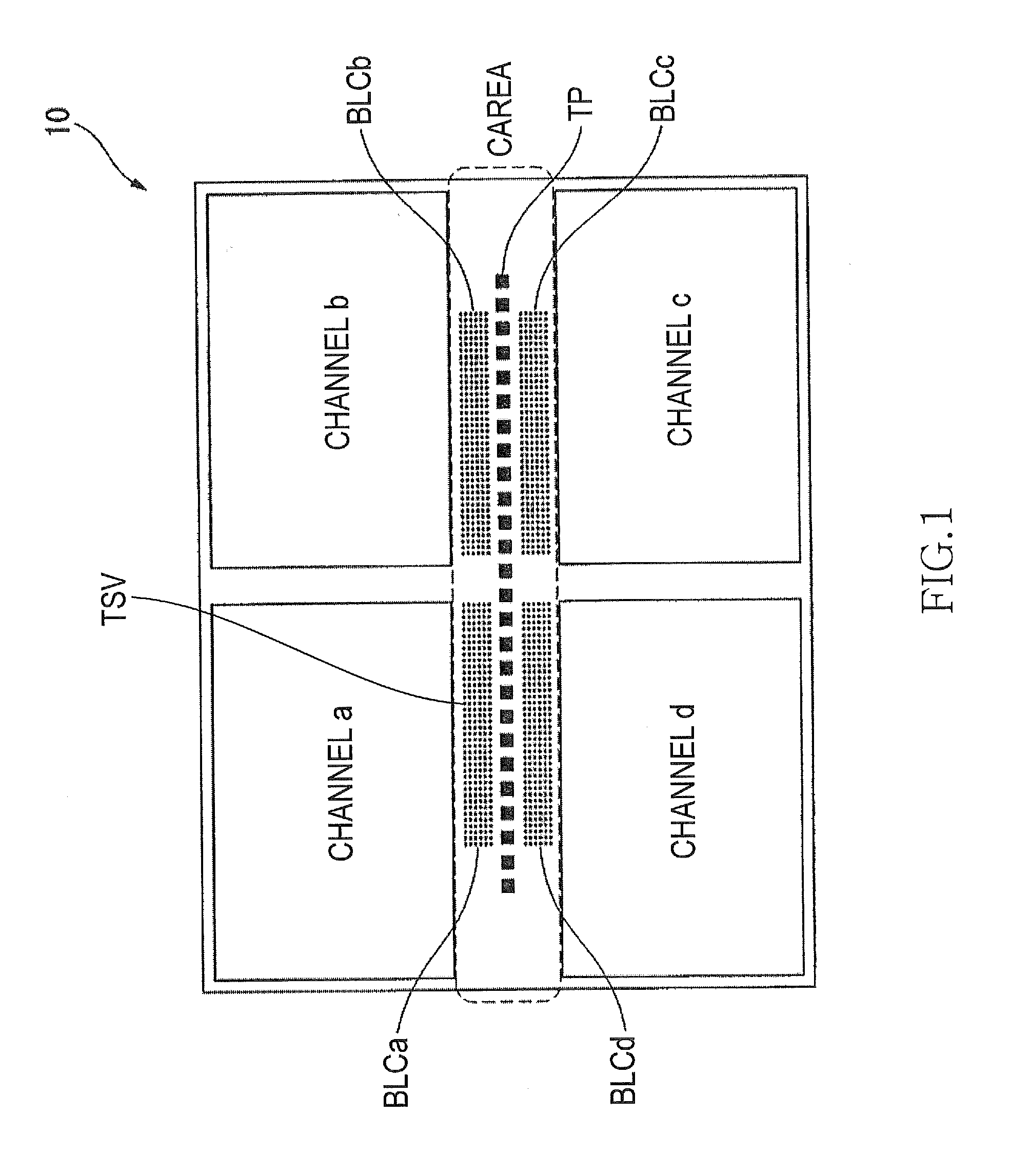
[0022]Referring now to FIG. 1, the semiconductor chip 10 includes four dynamic random access memories (DRAMs) having a volatile storing function which are arranged on a single semiconductor chip. The semiconductor chip 10 according to this embodiment is a memory chip, so-called wide I / O DRAM.

[0023]With such a configuration, channels a to d can transmit and receive data, commands, and addresses to / from outside the chip independently of each other. More specifically, the channels a to d can independently perform various types of operations such as a read operation, write operation, and refresh operation by using respective corresponding control circuits to be described later.

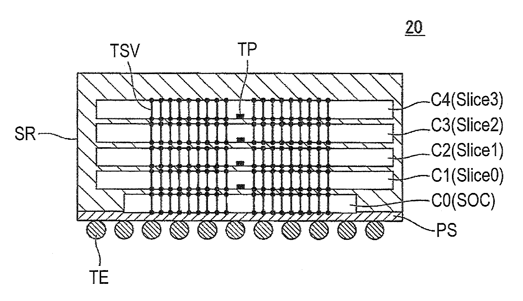
[0024]As shown in FIG. 1, a plurality of penetration electrodes TSV and test pads TP are arranged in the center area CAREA of the semiconductor chip 10. The plurality of penetr...


PUM


Abstract

Disclosed herein is a device that including a first chip having first to fourth terminals and a second chip having fifth to seventh terminals. The first chip further includes a penetration electrode connected between the first and fourth electrodes and a first internal node coupled to of which an electrical potential being changed in response to an electrical potential of the first terminal. The second chip further includes a second internal node coupled to of which an electrical potential being changed in response to an electrical potential of the fifth terminal. The first internal node is electrically coupled to both the second terminal and the sixth terminal. The second internal node is electrically coupled to both the third terminal and the seventh terminal.

Description

BACKGROUND OF THE INVENTION[0001]1. Field of the Invention[0002]The present invention relates to a semiconductor device, and more particularly to a semiconductor device having a plurality of semiconductor chips.[0003]2. Description of Related Art[0004]In recent years, a semiconductor device of a stacked type has been well known. A semiconductor device of a stacked type includes a plurality of semiconductor chips that employ a plurality of penetration electrodes. The plurality of semiconductor chips are electrically connected via the penetration electrodes. According to this configuration, a plurality of the semiconductor chips can be packaged on the circuit substrate in high density.[0005]Such a stacked semiconductor device needs to be tested whether input terminals of the semiconductor chips for signals to be supplied in common are electrically connected to outside properly.[0006]In recent years, the number of input terminals of individual semiconductor chips in a stacked semicondu...

Claims


Application Information

Patent Timeline
IPC IPC(8): H01L23/498
CPCH01L23/49816H01L2224/16145H01L2224/16225H01L2924/15311H01L25/0657H01L23/481H01L2225/06517H01L2225/06596H01L2225/06513H01L2225/06541H01L25/18
Inventor WADA, SHOJIISHIKAWA, TORU
Owner LONGITUDE SEMICON S A R L
Features
  • R&D
  • Intellectual Property
  • Life Sciences
  • Materials
  • Tech Scout
  • Unparalleled Data Quality
  • Higher Quality Content
  • 60% Fewer Hallucinations
Learn More