

Optical image capturing lens system
- Summary
- Abstract
- Description
- Claims
- Application Information
AI Technical Summary
Benefits of technology
Problems solved by technology
Method used
Image

Examples
1st embodiment
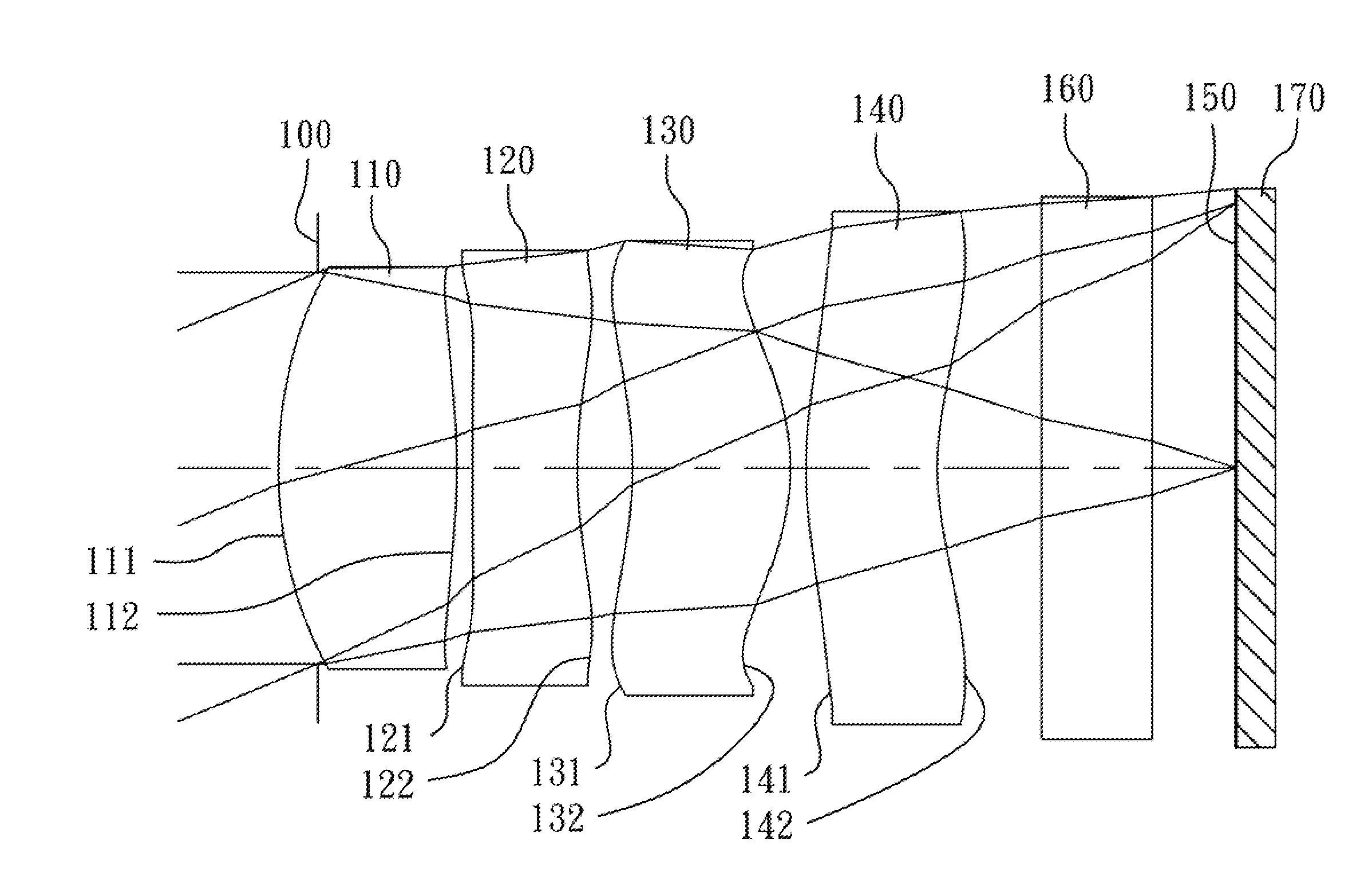
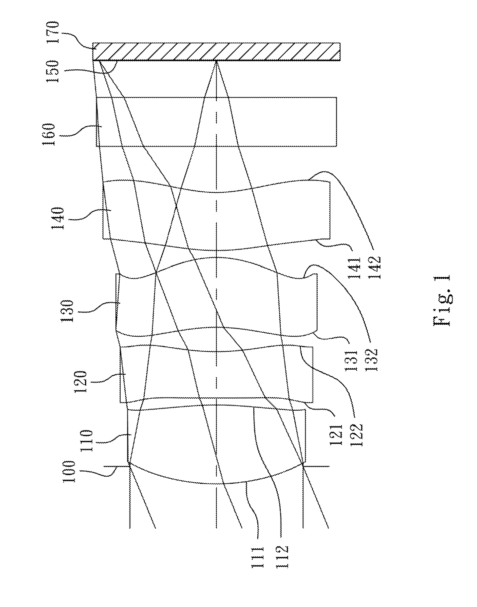
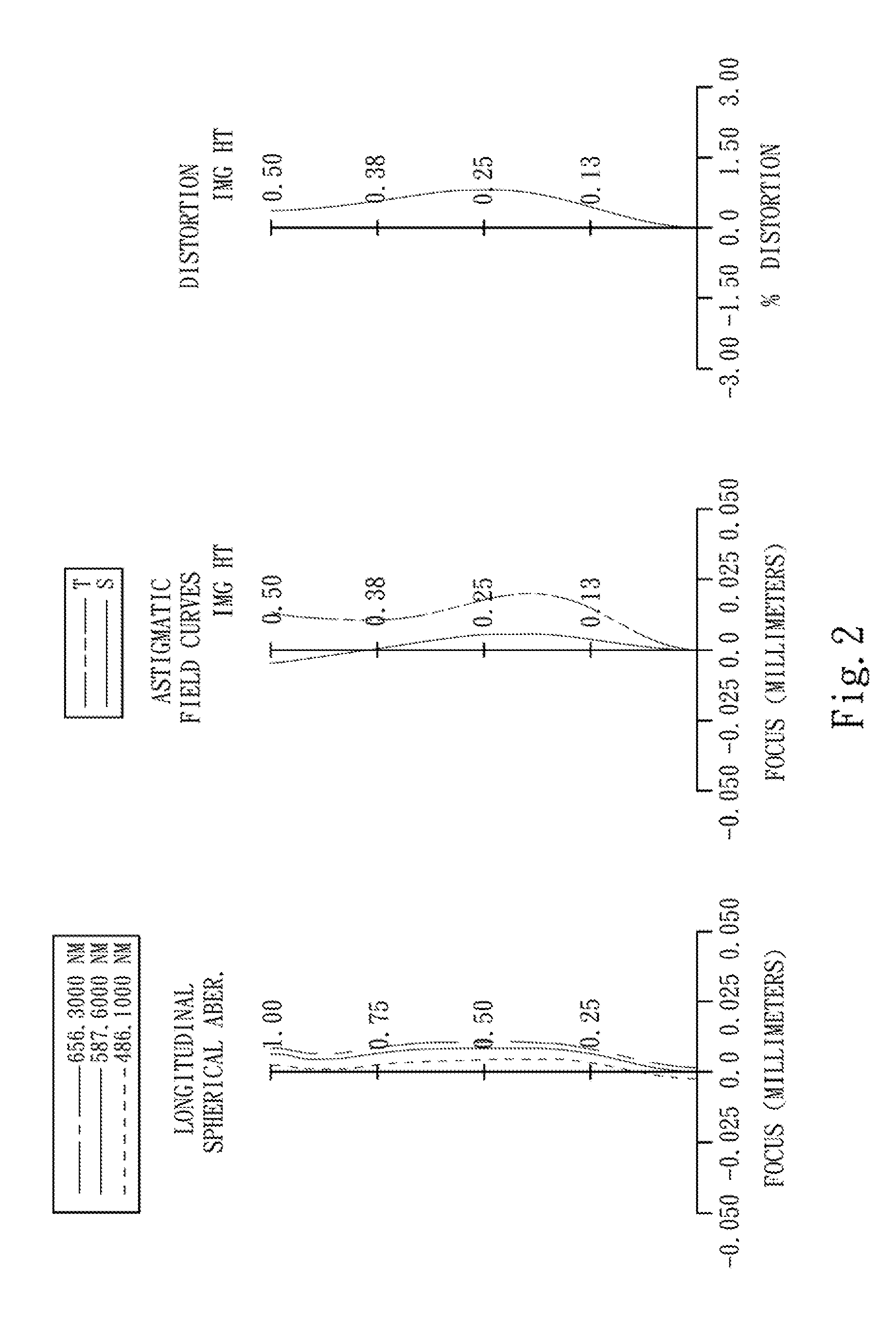
[0073]FIG. 1 is a schematic view of an optical image capturing lens system according to the 1st embodiment of the present disclosure. FIG. 2 shows spherical aberration curves, astigmatic field curves and a distortion curve of the optical image capturing lens system according to the 1st embodiment. FIG. 3 shows relationship diagrams of spatial frequency-diffraction limit value and spatial frequency-field modulation transfer function value according to the 1st embodiment. In FIG. 1, the optical image capturing lens system includes, in order from an object side to an image side, an aperture stop 100, a first lens element 110, a second lens element 120, a third lens element 130, a fourth lens element 140, an IR-filter 160, an image plane 150 and an image sensor 170.
[0074]The first lens element 110 with positive refractive power has a convex object-side surface 111 and a convex image-side surface 112, and is made of plastic material. The object-side surface 111 and the image-side surface...
2nd embodiment
[0102]FIG. 4 is a schematic view of an optical image capturing lens system according to the 2nd embodiment of the present disclosure. FIG. 5 shows spherical aberration curves, astigmatic field curves and a distortion curve of the optical image capturing lens system according to the 2nd embodiment. FIG. 6 shows relationship diagrams of spatial frequency-diffraction limit value and spatial frequency-field modulation transfer function value according to the 2nd embodiment. In FIG. 4, the optical image capturing lens system includes, in order from an object side to an image side, an aperture stop 200 a first lens element 210, a second lens element 220, a third lens element 230, a fourth lens element 240, an IR-filter 260, an image plane 250 and an image sensor 270.
[0103]The first lens element 210 with positive refractive power has a convex object-side surface 211 and a convex image-side surface 212, and is made of plastic material. The object-side surface 211 and the mage-side surface 2...
3rd embodiment
[0110]FIG. 7 is a schematic view of an optical image capturing lens system according to the 3rd embodiment of the present disclosure. FIG. 8 shows spherical aberration curves, astigmatic field curves and a distortion curve of the optical image capturing lens system according to the 3rd embodiment. FIG. 9 shows relationship diagrams of spatial frequency-diffraction limit value and spatial frequency-field modulation transfer function value according to the 3rd embodiment. In FIG. 7, the optical image capturing lens system includes, in order from an object side to an image side, a first lens element 310, an aperture stop 300, a second lens element 320, a third lens element 330, a fourth lens element 340, an IR-filter 360, an image plane 350 and an image sensor 370.
[0111]The first lens element 310 with positive refractive power has a convex object-side surface 311 and a convex image-side surface 312, and is made of plastic material. The object-side surface 311 and the image-side surface...
PUM
 Abstract
Description
Claims
Application Information