Touch surface and method of manufacturing same

Inactive Publication Date: 2013-07-18
NANOMADE CONCEPT +2
View PDF4 Cites 12 Cited by
  • Summary
  • Abstract
  • Description
  • Claims
  • Application Information

AI Technical Summary

Benefits of technology

The invention is a device that uses nanoparticles to measure force on a rigid surface. It allows for flexibility in the shape and nature of the touch surface, and measures the electrical properties of the nanoparticles assembly using a resonant circuit. This means that the device can measure without contact, using electromagnetic excitation. The technical effect is improved accuracy and flexibility in measuring force on a rigid surface.

Problems solved by technology

The touch surfaces of the prior art can primarily detect the contact, but cannot quantify it.
However, the difficulty with this method lies in several aspects.
As an example, while it is easy to determine by reverse method the loading mode of a thin flat test specimen held by its periphery when the forces normal to this plane are applied at points sufficiently far from the edges, it becomes significantly more complicated to apply such a method if the surface of the test specimen is curved or if it is held in a more complex way.
However, this principle suffers from the same limitations as the other technologies of the prior art, namely that the touch function, i.e. the ability to measure an action essentially normal to the surface, is dependent on boundary conditions, on the shape of the test specimen and on the ability to evaluate the latter's stressing by reverse method, the gages measuring the deformations tangential to the functionalized surface.

Method used


Image

  • Touch surface and method of manufacturing same
  • Touch surface and method of manufacturing same
  • Touch surface and method of manufacturing same

Examples


second embodiment

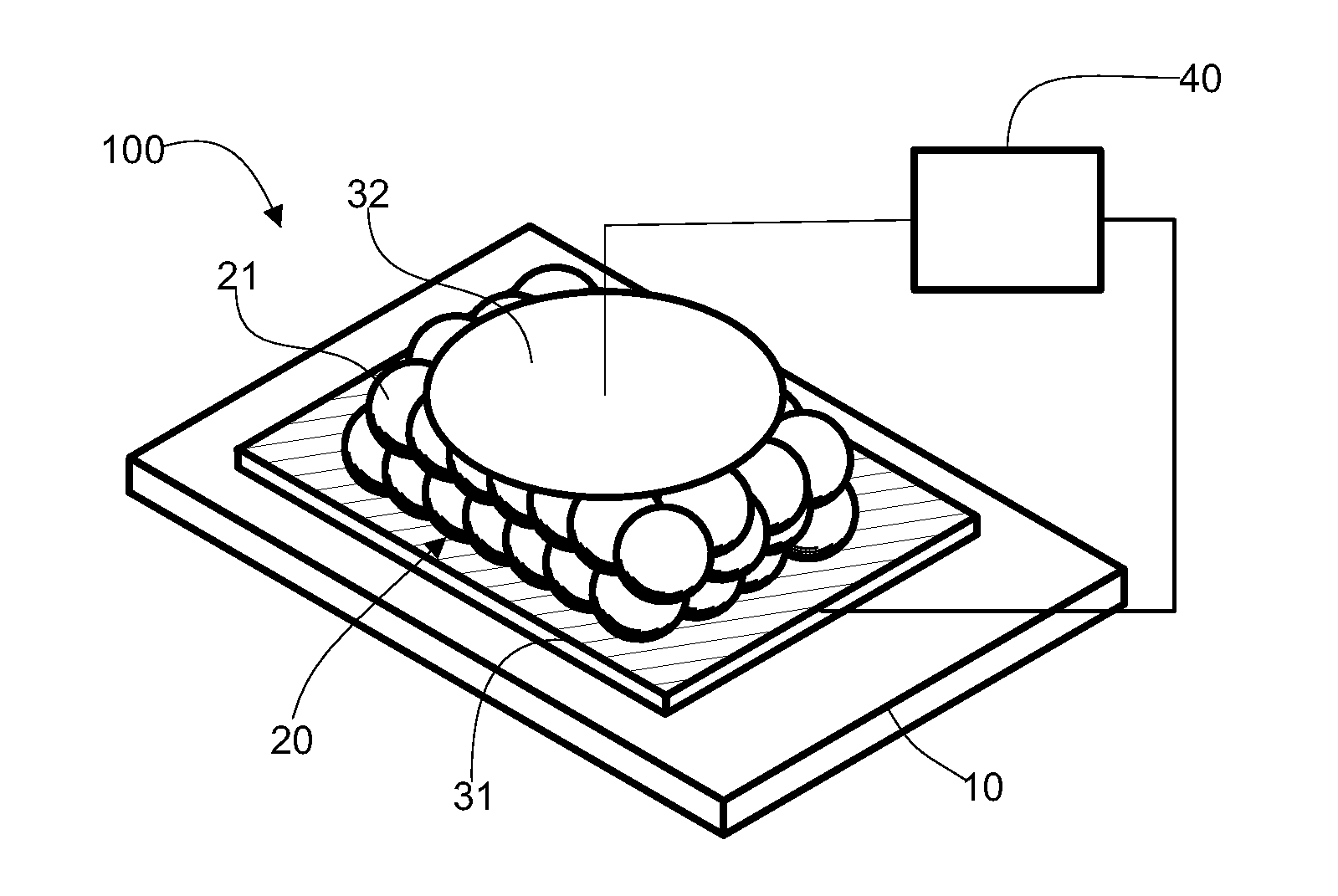
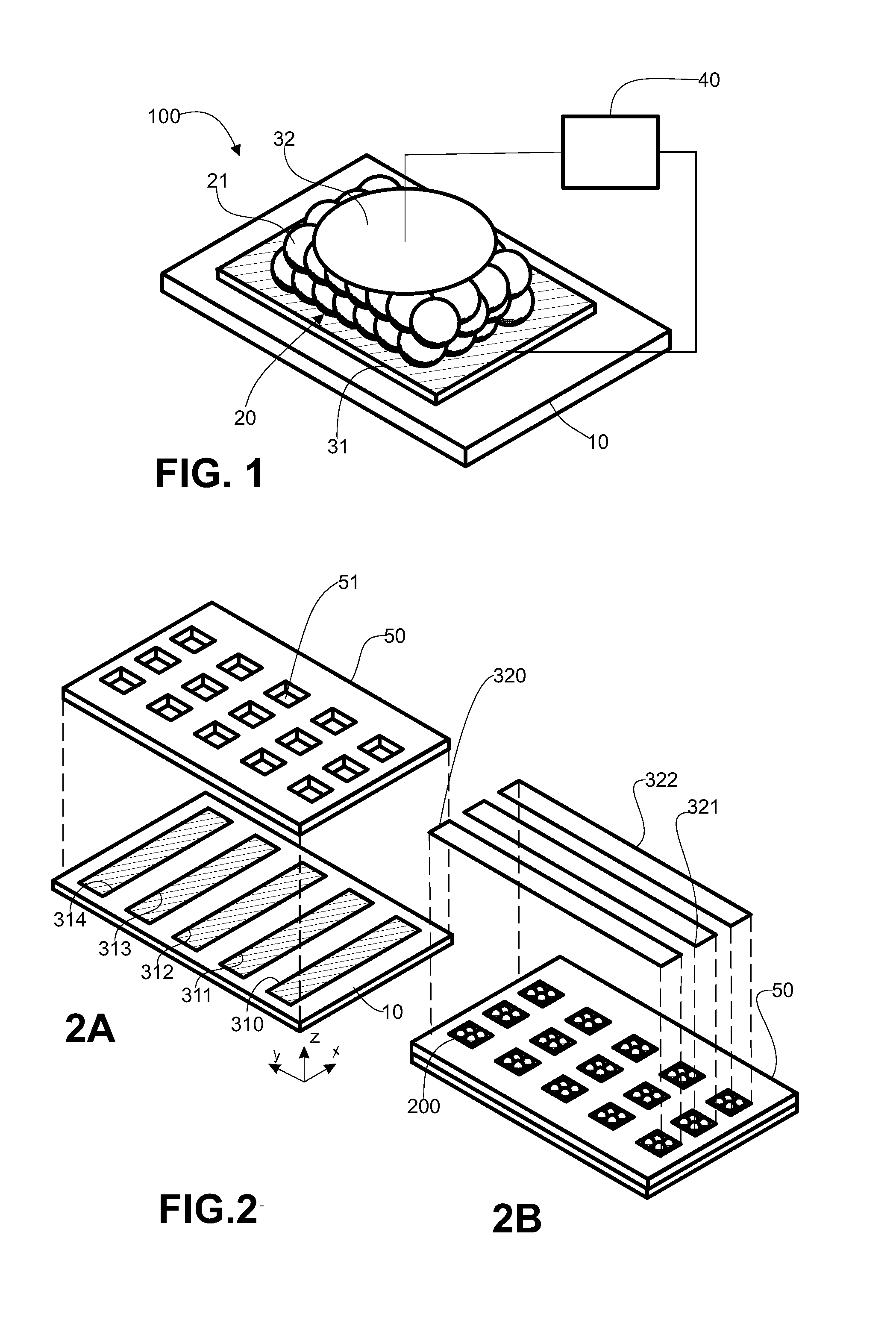
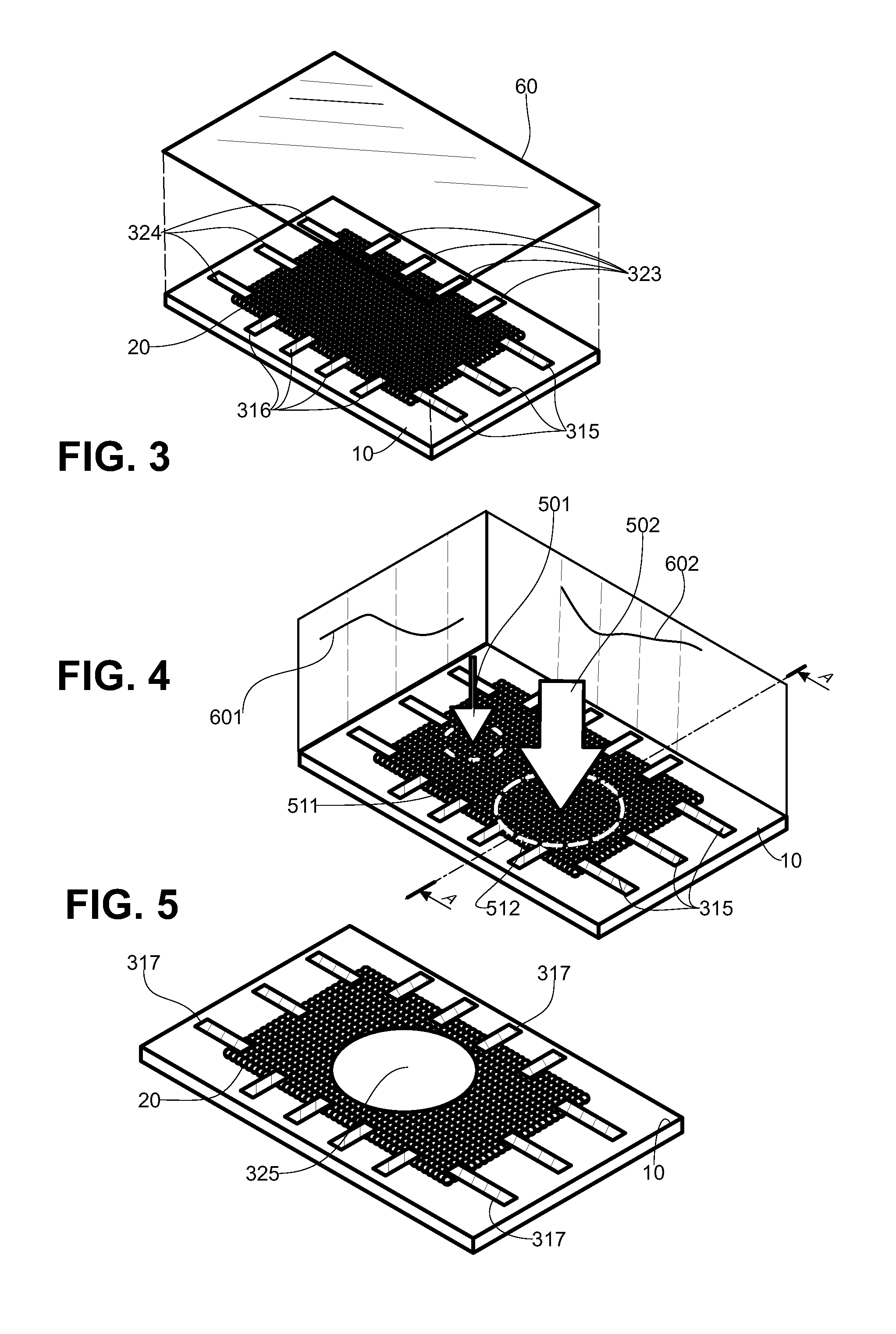
[0076]FIG. 3: the device that is the subject of the invention comprises an insulating substrate (10), on which is deposited a nanoparticles assembly (20) covering most of its surface. Said nanoparticles assembly can be single-layered or comprise several layers superimposed in a direction normal to the surface of the substrate (10).

[0077]A first ensemble of conductive strips (315, 316) is deposited on the substrate so as to form the first electrode, such that said strips extend between a portion of the substrate not covered by the nanoparticles assembly and said assembly in contact with the latter. A second ensemble of strips (323, 324), forming the second electrode, is deposited in the same way as the first strips, in symmetry with them in relation to the center of the center of the nanoparticles assembly. Finally, an insulating film (60) is deposited over everything.

[0078]FIG. 6: according to a variant of this embodiment, the discrete strips forming the first electrode are grouped...

third embodiment

[0080]FIG. 5: the device that is the subject of the invention comprises an insulating substrate (10) on which a nanoparticles assembly (20) covering a portion of the surface of said substrate is deposited. The first electrode is formed of an ensemble of strips (317) deposited on the substrate and extending between a portion of the substrate that is not covered and the nanoparticles assembly (20), in contact with the latter. The second electrode (325) is placed on the nanoparticles assembly, the ensemble being covered by an insulating film (not shown). When a force is applied to the second electrode (325), both the normal and tangential components of said force change the distance between the nanoparticles of the assembly (20). The point of application of the force being known, i.e. substantially at the center of the second electrode (325), measuring an electrical property between said second electrode (325) and each of the strips (317) forming the first electrode makes it possible ...


PUM


Abstract

A device for detecting and quantifying a force applied on a surface comprising a test specimen, an electrically insulating substrate, a first electrode bound to the substrate, a second electrode, an assembly of conductive or semi-conductive nanoparticles in contact with the two electrodes, and a measurement device. The measurement device provides proportional information with respect to an electrical property of the nanoparticles assembly. The electrical property is measured between the first and second electrode. The test specimen is the nanoparticles assembly itself and the electrical property is sensitive to the distance between the nanoparticles of the assembly. The invention uses the nanoparticles assembly itself as a test specimen and allows a force to be quantified even if the nanoparticles assembly is deposited on a rigid substrate.

Description

RELATED APPLICATIONS[0001]This application is a §371 application from PCT / EP2011 / 063205 filed Aug. 1, 2011, which claims priority from French Patent Application No. 10 56387 filed Aug. 2, 2010, each of which is herein incorporated by reference in its entirety.TECHNICAL FIELD OF INVENTION[0002]The invention belongs to the field of touch surfaces and relates to such a surface, its method of realization and its use for detecting and measuring forces applied on such a surface. This type of surface is used, for example, in many mass-market electronic applications, in particular computer applications, under different forms, called “touch pad”, “touch screen”, “write pad”, etc.BACKGROUND OF THE INVENTION[0003]In these examples of the prior art, the touch surfaces are configured so as to detect one or more contacts, which can be from a finger or by means of an accessory such as a stylus. When they comprise a plurality of sensors arranged according to a matrix organization, they allow the mo...

Claims


Application Information

Patent Timeline
IPC IPC(8): G01R27/02G01R27/26
CPCG01L1/146G01L1/205G06F3/041G01R27/2605G06F3/044G06F3/045G01R27/02G06F3/0414G06F3/0416G06F3/0445G06F3/0447G01L1/144G06F2203/04103G06F2203/04105G06F1/16
Inventor VIALLET, BENO TRESSIER, LAURENCEGRISOLIA, JEREMIESONGEON, LIONELMOUCHEL LA FOSSE, ERICCZORNOMAZ, LUKAS
Owner NANOMADE CONCEPT
Why Eureka
Try Eureka