External auxiliary execution unit interface to off-chip auxiliary execution unit

a technology of auxiliary execution unit and external auxiliary, which is applied in the field of data processing, can solve the problems of increasing complexity and power of microprocessors, microcontrollers, microcontrollers, etc., and reducing power consumption and feature sizes, cost, power consumption and other issues

Active Publication Date: 2013-07-18
IBM CORP
View PDF6 Cites 21 Cited by
  • Summary
  • Abstract
  • Description
  • Claims
  • Application Information

AI Technical Summary

Benefits of technology

[0010]The invention addresses these and other problems associated with the prior art by providing a method, apparatus, and program product that utilize an external Auxiliary Execution Unit (AXU) interface between a processing core disposed in a first programmable chip and an off-chip AXU disposed in a second programmable chip. The AXU interface integrates an AXU with a processing core that includes at least an issue unit and a fixed point execution unit, and enables the issue unit to issue instructions to the AXU in much the same manner as the issue unit would be able to issue instructions to an AXU that was disposed on the same chip. By doing so, the AXU on the second programmable chip can be designed, tested and verified independent of the processing core on the first programmable chip, thereby enabling a common processing core, which has been designed, tested, and verified, to be used in connection with multiple different AXU designs.

Problems solved by technology

Programmable chips such as microprocessors, microcontrollers, Application Specific Integrated Circuits (ASIC's) and the like continue to increase in complexity and power while costs, power consumption and feature sizes decrease.
Moreover, once a particular chip design has been developed, tested and verified, manufacturing costs are often comparatively low on a per unit basis.
On the other hand, given the substantial up-front efforts still required to design, test and verify multiple functional units integrated into application-specific programmable chips, there are still substantial costs associated with bringing application-specific programmable chips to market.
Customers often rely on other entities to design their programmable chips, and often designs that are proprietary to both the entities that design the programmable chips and the customers are integrated together on the same programmable chips, often leading to licensing issues as well as concerns about maintaining the confidential nature of some designs.

Method used


Image

  • External auxiliary execution unit interface to off-chip auxiliary execution unit
  • External auxiliary execution unit interface to off-chip auxiliary execution unit
  • External auxiliary execution unit interface to off-chip auxiliary execution unit

Examples


Embodiment Construction

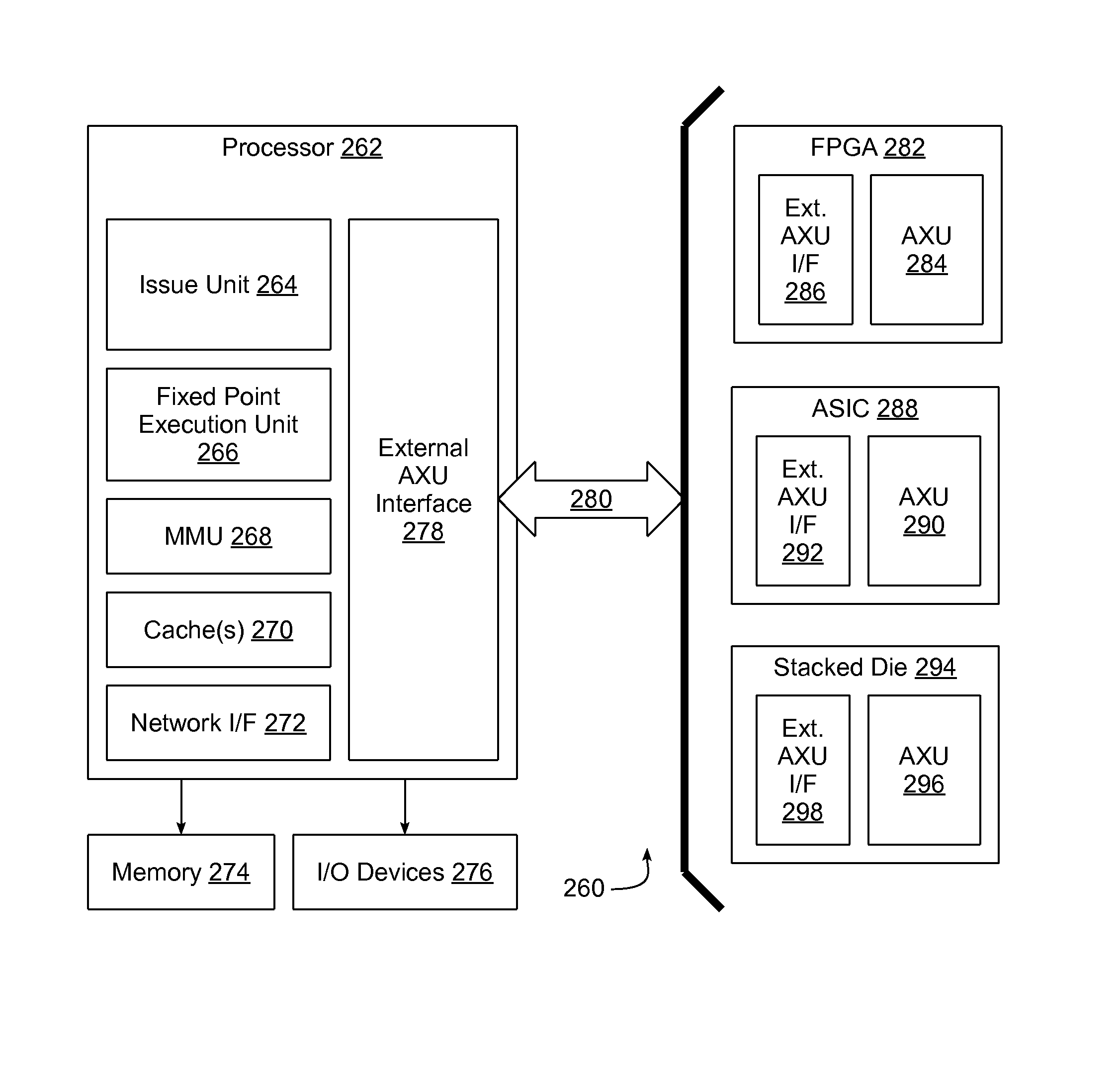
[0022]Embodiments consistent with the invention utilize an external Auxiliary Execution Unit (AXU) interface between a processing core disposed in a first programmable chip and an off-chip AXU disposed in a second programmable chip to integrate the AXU with an issue unit, a fixed point execution unit, and optionally other functional units in the processing core. The external AXU interface enables the issue unit to issue instructions to the AXU in much the same manner as the issue unit would be able to issue instructions to an AXU that was disposed on the same chip. By doing so, the AXU on the second programmable chip can be designed, tested and verified independent of the processing core on the first programmable chip, thereby enabling a common processing core, which has been designed, tested, and verified, to be used in connection with multiple different AXU designs.

[0023]An AXU consistent with the invention may incorporate various types of functionality that extends, accelerates o...


PUM


Abstract

An external Auxiliary Execution Unit (AXU) interface is provided between a processing core disposed in a first programmable chip and an off-chip AXU disposed in a second programmable chip to integrate the AXU with an issue unit, a fixed point execution unit, and optionally other functional units in the processing core. The external AXU interface enables the issue unit to issue instructions to the AXU in much the same manner as the issue unit would be able to issue instructions to an AXU that was disposed on the same chip. By doing so, the AXU on the second programmable chip can be designed, tested and verified independent of the processing core on the first programmable chip, thereby enabling a common processing core, which has been designed, tested, and verified, to be used in connection with multiple different AXU designs.

Description

FIELD OF THE INVENTION[0001]The invention is generally related to data processing, and in particular to processor architectures and execution units incorporated therein.BACKGROUND OF THE INVENTION[0002]Computers and other programmable electronic devices continue to be integrated into every aspect of society. Whereas computers once occupied entire rooms, computers and the integrated circuit devices, or chips, that power such computers have now been miniaturized and commoditized to such an extent that they can be found in even the most mundane of products and devices.[0003]Programmable chips such as microprocessors, microcontrollers, Application Specific Integrated Circuits (ASIC's) and the like continue to increase in complexity and power while costs, power consumption and feature sizes decrease. Whereas computers once incorporate separate chips for processors, graphics controllers, coprocessors, memory controllers, and other chipset logic, oftentimes all of these types of functional...

Claims


Application Information

Patent Timeline
Patent Type & Authority Applications(United States)
IPC IPC(8): G06F9/30
CPCG06F9/3877G06F15/8038G06F9/3881G06F15/7864G06F13/12
Inventor MEJDRICH, ERIC O.SCHARDT, PAUL E.SHEARER, ROBERT A.SWENSON, COREY V.
Owner IBM CORP
Why Eureka
Try Eureka