Supercharge Your Innovation With Domain-Expert AI Agents!

Embedded circuit in a MEMS device

a technology of embedded circuits and mems devices, applied in the field of acoustic devices, can solve the problems of increasing user dissatisfaction with the previous approach, reducing the size of devices,

Active Publication Date: 2013-08-01
KNOWLES ELECTRONICS INC
View PDF2 Cites 71 Cited by
  • Summary
  • Abstract
  • Description
  • Claims
  • Application Information

AI Technical Summary

Benefits of technology

The patent text describes a method of embedding a circuit in a MEMS device to reduce its size. The circuit is placed on a printed circuit board and its signals are routed directly to the outer layer of metallization, which is used for final assembly. This approach allows for a smaller device size and reduces the impact of previous limitations on reducing the size of the device. The technical effect is to provide a more efficient solution for embedding integrated circuits in MEMS devices to achieve smaller sizes.

Problems solved by technology

In many applications, the size of the MEMS device is desired to be as small as possible and the above-mentioned layout of these devices has caused problems in reducing the size of devices.
Because of these shortcomings, previous approaches have not adequately addressed the above-mentioned problems and user dissatisfaction with these previous approaches has increased.

Method used


Image

  • Embedded circuit in a MEMS device
  • Embedded circuit in a MEMS device
  • Embedded circuit in a MEMS device

Examples


Embodiment Construction

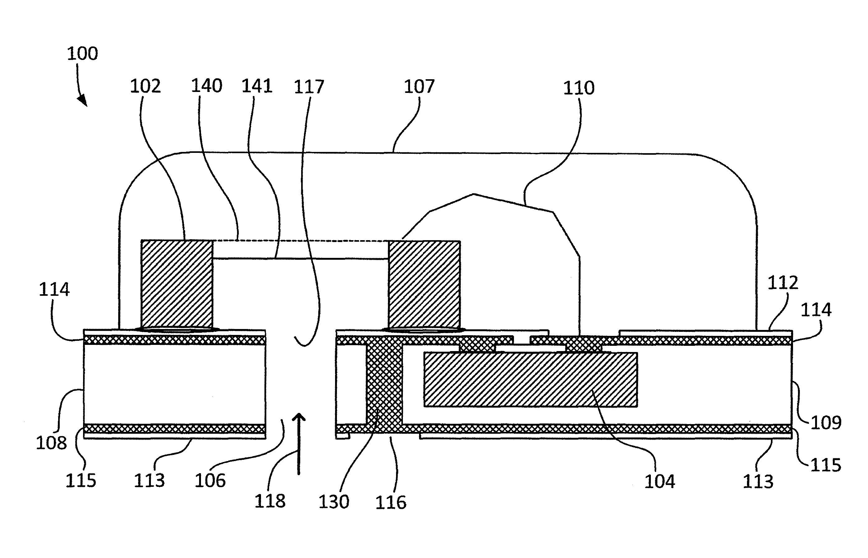
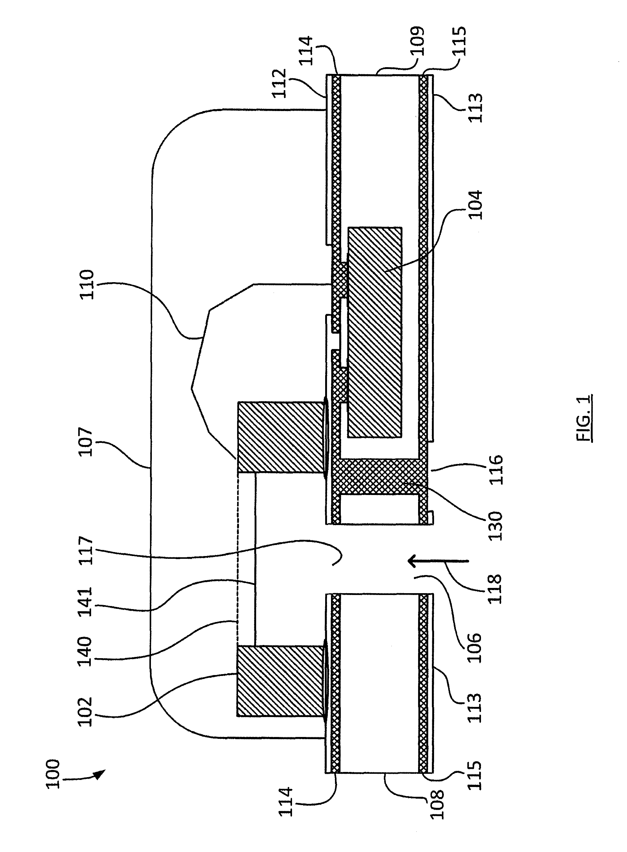
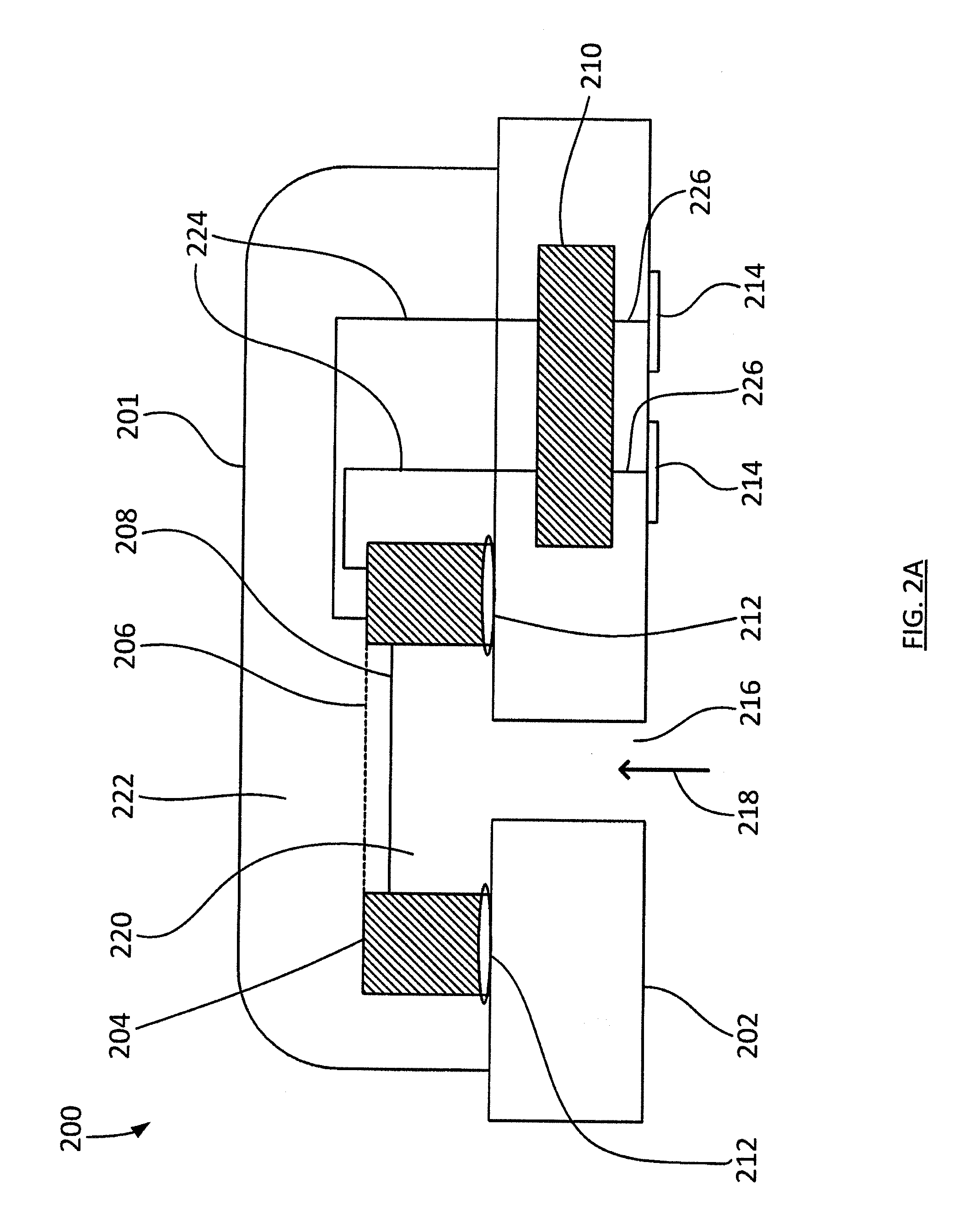
[0014]Approaches are provided where an integrated circuit (e.g., an ASIC or similar device) or other electrical circuit component is embedded in the printed circuit board (PCB) of an acoustic device or assembly (e.g., a MEMS microphone). As used herein, the integrated circuit is an electronic device that may be enclosed in its own separate housing and performs separate processing functions on an incoming electrical signal where the processing functions are more than merely passing the signal. In other words, the integrated circuit is more than just a transmission medium.

[0015]In some of these embodiments, the output signals of the embedded integrated circuit (e.g., the ASIC) are routed directly into plated through hole vias in the PCB to an outer layer of metallization to customer solder pads (e.g., at the “bottom side” of the PCB). Additionally, the signals between the ASIC and MEMS die are routed directly into plated through hole vias in the PCB to the outer layer metallization op...


PUM

PropertyMeasurementUnit
Volumeaaaaaaaaaa
Electrical conductoraaaaaaaaaa

Abstract

A Microelectromechanical System (MEMS) microphone includes a printed circuit board, a MEMS die, and an integrated circuit. The MEMS die is disposed on a top surface of the printed circuit board. The integrated circuit is disposed at least partially within the printed circuit board and produces at least one output signal. The output signals of the integrated circuit are routed directly into at least one conductor to access pads at the printed circuit board and the access pads are disposed on a bottom surface of the printed circuit board that is opposite the top surface.

Description

CROSS REFERENCES TO RELATED APPLICATIONS[0001]This patent claims benefit under 35 U.S.C. §119 (e) to U.S. Provisional Application No. 61 / 593,611 entitled “Embedded Circuit In A MEMS Device” filed Feb. 1, 2012, the content of which is incorporated herein by reference in its entirety.[0002]This patent also claims benefit under 35 U.S.C. §119 (e) to U.S. Provisional Application No. 61 / 706,350 entitled “Embedded Circuit In A MEMS Device” filed Sep. 27, 2012, the content of which is incorporated herein by reference in its entirety.TECHNICAL FIELD[0003]This application relates to acoustic devices and, more specifically, to the disposition of integrated circuits at or within these devices.BACKGROUND OF THE INVENTION[0004]MicroElectroMechanical System (MEMS) devices include microphones and speakers to mention two examples. In the case of a MEMS microphone, sound energy enters through a sound port and vibrates a diaphragm and this action creates a corresponding change in electrical potential...

Claims


Application Information

Patent Timeline
IPC IPC(8): B81B3/00
CPCH04R19/005B81C1/0023B81B3/0064H01L2924/181H01L2224/16225H01L2224/32225H01L2224/48091H01L2224/48227H01L2224/73265H01L2924/10155H01L2924/15151Y10T29/49005H01L2924/00012H01L2924/00014H01L2924/00
Inventor VOS, SANDRA F.GIESECKE, DANIEL
Owner KNOWLES ELECTRONICS INC
Features
  • R&D
  • Intellectual Property
  • Life Sciences
  • Materials
  • Tech Scout
  • Unparalleled Data Quality
  • Higher Quality Content
  • 60% Fewer Hallucinations
Learn More