Biometric Scanner Having A Protective Conductive Array

a biometric scanner and array technology, applied in the field of biometric scanners, can solve the problems of prone to mechanical abuse and damage, prone to damage, and especially susceptible to damage, and the existing ef/c biometric scanners are susceptible to damag

Active Publication Date: 2013-08-08
QUALCOMM INC
View PDF8 Cites 39 Cited by
  • Summary
  • Abstract
  • Description
  • Claims
  • Application Information

AI Technical Summary

Benefits of technology

[0009]The sensor may have a plurality of sensor electrodes, and in such an arrangement, the strands may be arranged to have a pitch that is smaller than the pitch of the sensor electrodes. For example, the pitch of the strands may be not greater than half the pitch of the sensor electrodes.

Problems solved by technology

Existing EF / C Biometric Scanners are susceptible to damage caused by mechanical abrasion and electrostatic discharge (“ESD”).
Capacitance and electric field sensors are, however, prone to mechanical abuse and damage, and they are especially susceptible to damage from ESD.

Method used


Image

  • Biometric Scanner Having A Protective Conductive Array
  • Biometric Scanner Having A Protective Conductive Array

Examples


Embodiment Construction

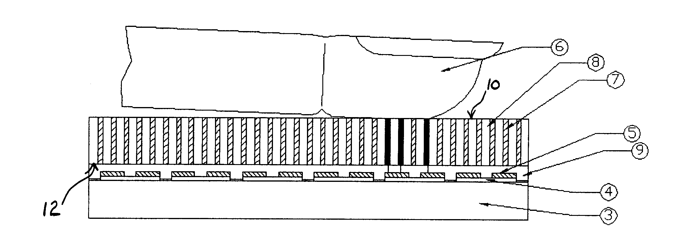
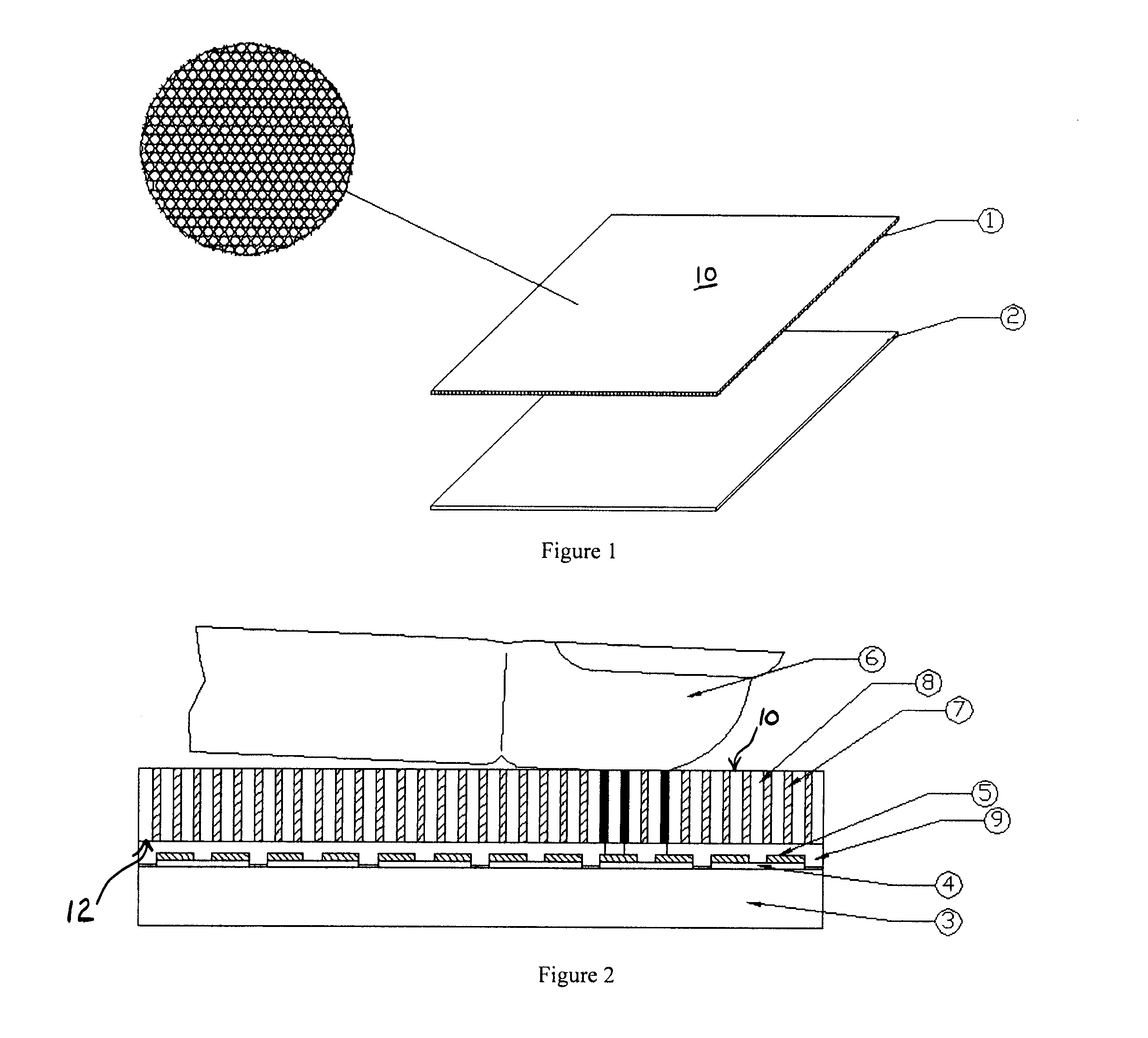
[0025]The invention may be employed to simultaneously protect a biometric scanner, such as a fingerprint scanner, from mechanical abuse and ESD, while allowing for interactive communication between the biometric scanner and a user. For example, the invention may provide a means of isolating the capacitance and / or electric field sensor through the use of a CS Array.

[0026]In an embodiment of the invention, conductive strands are placed between a sensor array and a user. In this manner, the user does not directly contact the sensor array, thereby preventing mechanical abrasion of the sensor array while allowing an electrical connection between the user and the sensor array to occur. A plurality of the conductive strands may be provided in the form of a CS Array.

[0027]The CS Array may be formed by placing an insulating matrix between the strands so that anisotropic conduction between a first primary surface and a second primary surface of the CS Array is the primary means of conduction ...


PUM


Abstract

A biometric scanner having a sensor and an array of conductive strands is disclosed. The sensor has at least one sensor electrode, and that sensor electrode may be a capacitance sensor, an electric field sensor, or an electroluminescent sensor. The array may have an electrical insulating material between adjacent ones of the conductive strands. The array serves to protect the sensor, and conduct through the array information about the electrical characteristics of a biometric object.

Description

CROSS-REFERENCE TO RELATED APPLICATION[0001]This application claims the benefit of priority to U.S. provisional patent application Ser. No. 61 / 595,335, filed on Feb. 6, 2012.FIELD OF THE INVENTION[0002]The present invention relates to biometric scanners that sense electrical characteristics of the biometric object (such as a finger) in order to obtain information about the biometric object.BACKGROUND OF THE INVENTION[0003]Since the 1800's biometric information has been collected from human fingers and hands by means of ink and paper. For the purposes of this document, the term fingerprint is used to mean the skin surface friction ridge detail of a single fingerprint, partial fingerprint or any portion of the skin surface friction ridge of up to and including the entire hand or foot. In recent years various electronic fingerprint scanning systems have been developed utilizing optical, capacitance, electric field, direct pressure, thermal, and acoustic methods. Methods based upon acou...

Claims


Application Information

Patent Timeline
Patent Type & Authority Applications(United States)
IPC IPC(8): G06F3/044
CPCG06F3/044G06K9/00053G06K9/0002G06V40/1329G06V40/1306
Inventor SCHNEIDER, JOHN K.KITCHENS, JACK C.
Owner QUALCOMM INC
Why Eureka
Try Eureka