Integrated circuit having a junctionless depletion-mode fet device

a technology of integrated circuits and fet devices, which is applied in the direction of basic electric elements, semiconductor devices, electrical apparatus, etc., can solve the problems of excessive high temperature, method of production of integrated circuits, and inability to achieve very high integration densities

Inactive Publication Date: 2013-08-08
COMMISSARIAT A LENERGIE ATOMIQUE ET AUX ENERGIES ALTERNATIVES
View PDF1 Cites 183 Cited by
  • Summary
  • Abstract
  • Description
  • Claims
  • Application Information

AI Technical Summary

Problems solved by technology

Such an integrated circuit production method does not however enable very high integration densities to be obtained bearing in mind the alignment tolerances between the electronic devices of the different levels, which must be taken into account when rigidly connecting the different levels.
Such a method of production of integrated circuits poses problems, however, when it is desired to produce devices requiring the implementation of steps involving substantial thermal budgets, such as for example MOSFET transistors, above levels including electrical interconnections and/or other MOSFET transistors.
Such a thermal activation step must generally be implemented, in the case of silicon, at a temperature of above approximately 850° C. However, the presence of electrical interconnections under the active layer containing the dopants to be activated is incompatible with the implementation of such thermal activation, bearing in mind the excessively high temperatures which must be attained.
This incompatibility i

Method used


Image

  • Integrated circuit having a junctionless depletion-mode fet device
  • Integrated circuit having a junctionless depletion-mode fet device
  • Integrated circuit having a junctionless depletion-mode fet device

Examples


first embodiment

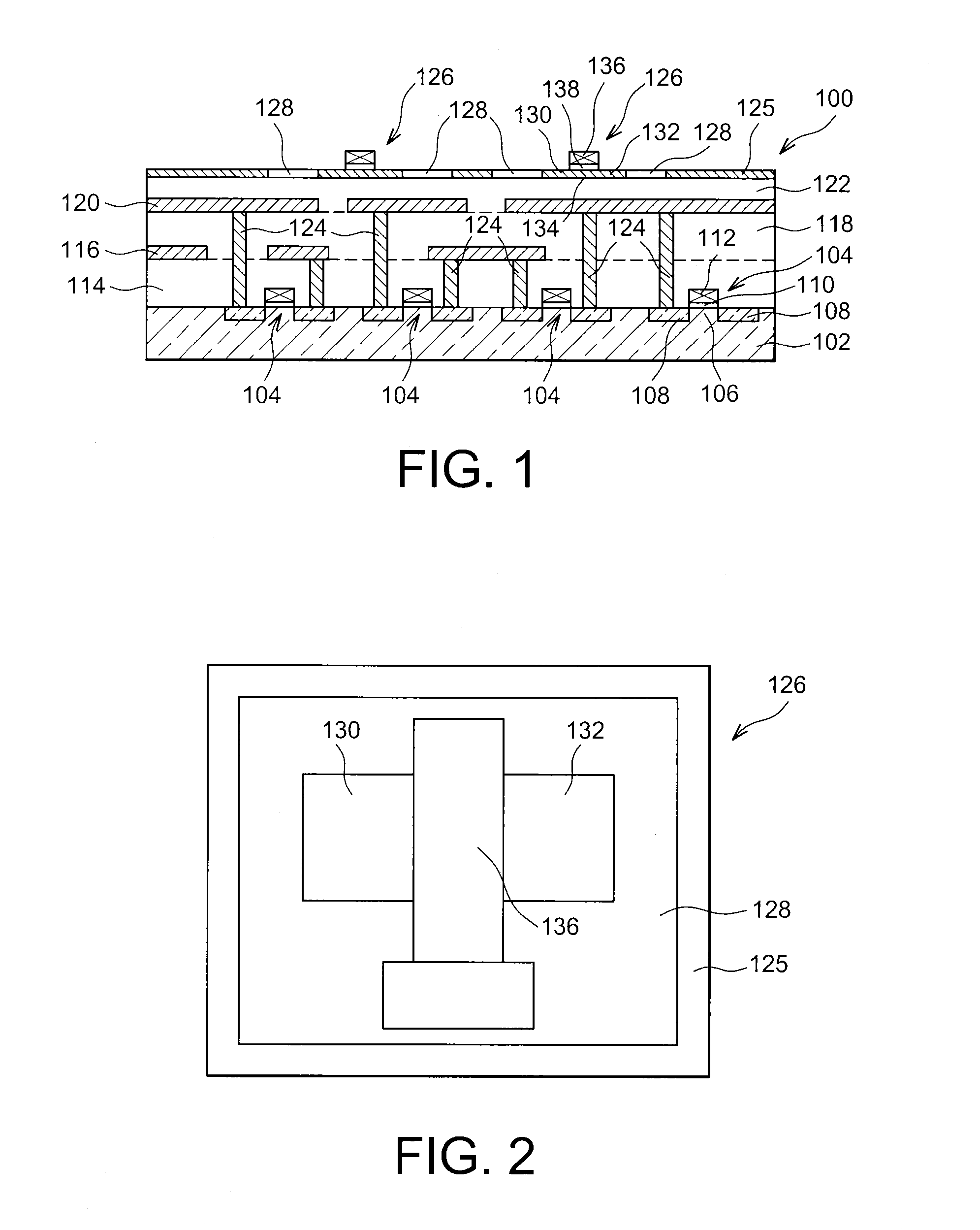
[0056]Reference is first made to FIG. 1, which represents an integrated circuit 100 with junctionless depletion-mode FET devices 126 according to a

[0057]Integrated circuit 100 includes a substrate 102, for example comprising a semiconductor such as silicon, and of the bulk type or SOI (silicon on insulator) type or FD-SOI (fully depleted silicon on insulator) type, or again of the PD-SOI (partially depleted silicon on insulator) type, in which MOSFET transistors 104 are produced. Each of these MOSFET transistors 104, for example of the nMOS type, has a P type channel area 106 and N+ type source and drain areas 108 formed in substrate 102. Channel 106 is topped by a gate dielectric 110 and a gate 112.

[0058]Substrate 102 and transistors 104 are covered by a first dielectric layer 114, for example made of SiO2, on which a first level of electrical interconnections 116 is formed. A second dielectric layer 118 covers first dielectric layer 114 and first level of electrical interconnectio...

second embodiment

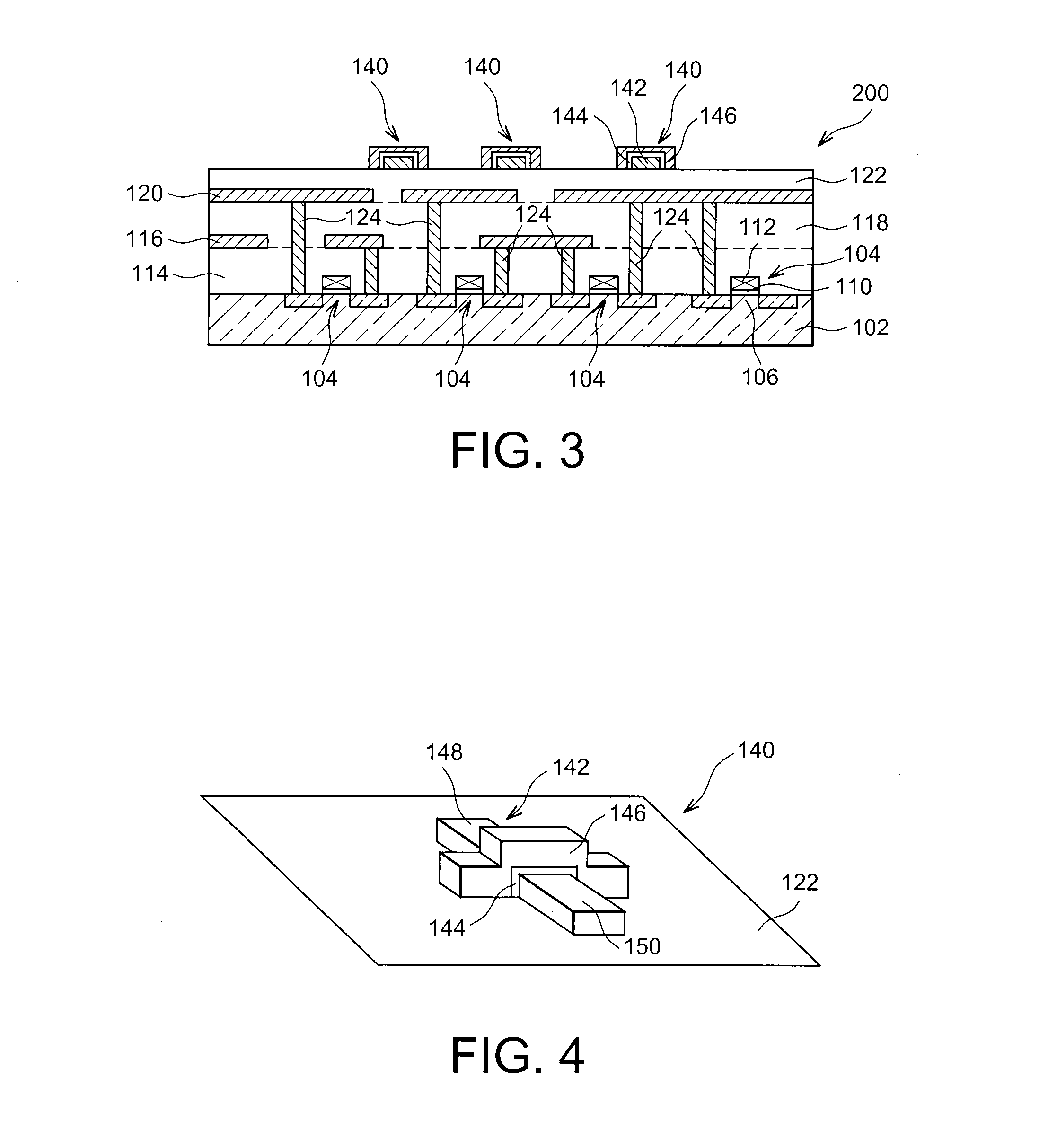
[0072]Reference is made to FIG. 3, which represents an integrated circuit 200 with junctionless depletion-mode FET devices 140 according to a Compared to integrated circuit 100, integrated circuit 200 includes junctionless depletion-mode FET transistors 140 which do not include parts of thin silicon layer 125 which are electrically insulated from the remainder of layer 125 by parts of dielectric material, but include uniformly doped silicon nanowires 142 obtained by etching in thin silicon layer 125. An example of such a junctionless depletion-mode FET transistor 140 is represented in FIG. 4. In this FIG. 4 a single nanowire 142 is represented. However, junctionless depletion-mode FET transistor 140 may include one or more nanowires 142. Nanowire 142 is partially covered by a gate dielectric 144 and by a gate 146, where the part of nanowire 142 located under gate dielectric 144 forms the channel of FET transistor 140. Nanowire 142 also forms a source 148 and a drain 150 of junction...

third embodiment

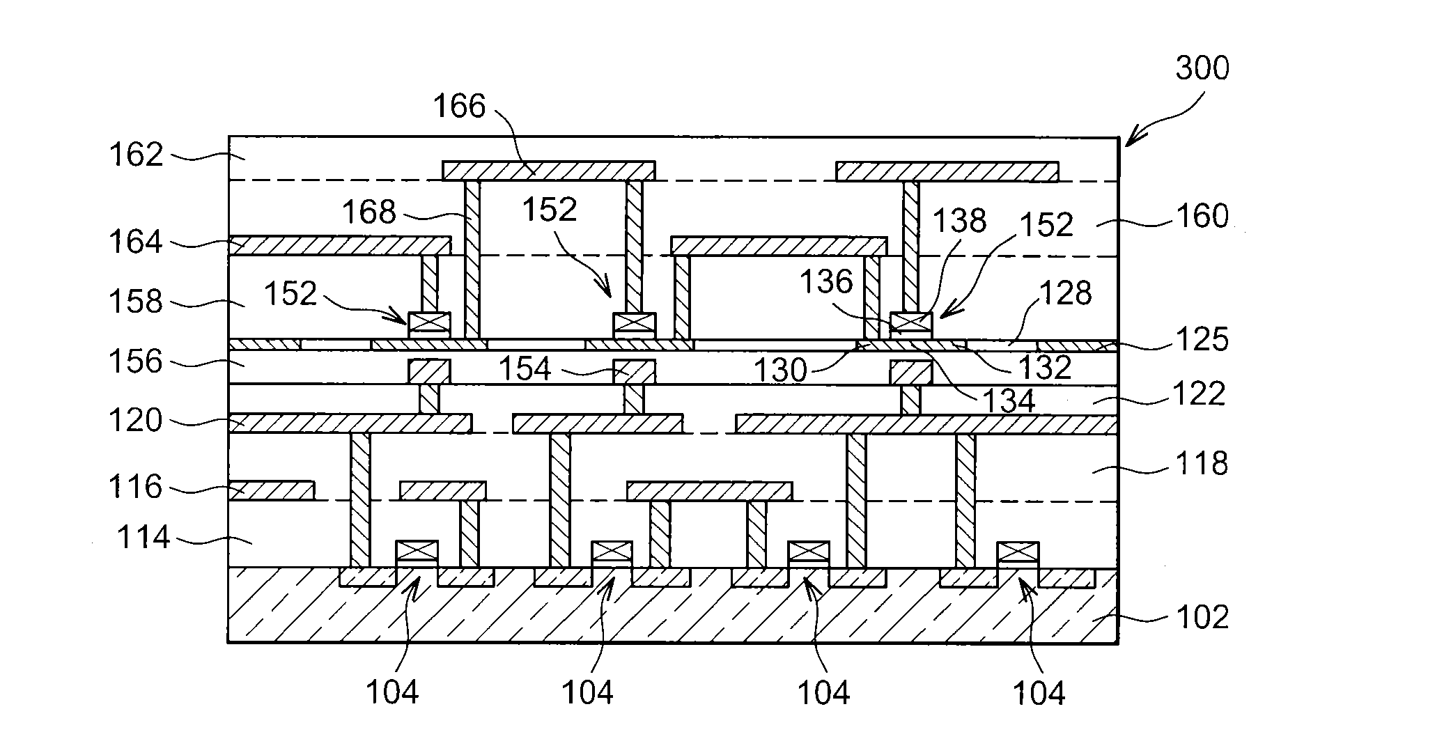
[0083]Reference is now made to FIG. 5, which represents an integrated circuit 300 with junctionless depletion-mode FET devices 152 according to a

[0084]Compared to integrated circuit 100 which was previously described in relation to FIG. 1, integrated circuit 300 includes junctionless depletion-mode FET transistors 152 which are different to previously described transistors 126. Indeed, compared to FET transistors 126, each of FET transistors 152 also includes a back gate positioned opposite channel 134 of transistor 152. These back gates 154 are produced using parts of electrically conductive material, for example metal, positioned on third dielectric layer 122 and covered by another dielectric layer 156 positioned between third dielectric layer 122 and thin silicon layer 125. Thin parts of dielectric layer 156 are sandwiched between back gates 154 and channel areas 134, forming back gate dielectrics. The operation of junctionless depletion-mode FET transistors 152 is comparable to ...


PUM


Abstract

A method for producing an integrated circuit, including, in this order: a) producing at least one MOS electronic circuit and/or at least one level of electrical interconnections on a substrate; b) uniformly implantating dopants in at least a portion of a layer of crystalline semiconductor; c) thermally activating the dopants implanted in the portion of the crystalline semiconductor layer; d) rigidly connecting the crystalline semiconductor layer to the substrate; and e) producing at least one junctionless depletion-mode FET device including a part of the portion of the crystalline semiconductor layer.

Description

TECHNICAL FIELD[0001]The invention relates to the field of integrated circuits, and more specifically that of three-dimensional integrated circuits, including several electronic levels superposed on one another, where each level includes one or more microelectronic devices such as field-effect transistors (FETs) and / or electrical interconnections. The invention also relates to a method of producing integrated circuit.[0002]The invention relates in particular to the production of very dense three-dimensional integrated circuits comprising several electronic levels, including microelectronic devices which are interconnected by levels of electrical interconnections.[0003]The invention has many applications in the fields of electronic using structures of the FET type, such as that of reconfigurable logics, three-dimensional static memories (SRAM), three-dimensional flash memories, addressing of memories, NEMS (electromechanical nanosystems) sensors, ChemFET chemical sensors, etc.STATE O...

Claims


Application Information

Patent Timeline
IPC IPC(8): H01L21/74
CPCH01L21/8221H01L27/0688H01L21/743H01L29/785H01L29/78696H01L27/11578H01L21/823807H10B43/20
Inventor ERNST, THOMASJAUD, MARIE-ANNEBATUDE, PERRINE
Owner COMMISSARIAT A LENERGIE ATOMIQUE ET AUX ENERGIES ALTERNATIVES
Why Eureka
Try Eureka